Scanning electron microscopes for quality control
Seth Price | January 07, 2025The scanning electron microscope (SEM) is a valuable tool for understanding what is happening to a material or biological sample at the sub-microscopic level. An SEM can be used to view objects at a higher resolution and at higher magnification than an optical (light) microscope, meaning finer details can be captured and understood.
SEMs are used heavily in the semiconductor, materials and metallurgical industries. They also can be used to provide information to biologists, forensic scientists and failure analysts, as subtle clues often lie in the smallest features.
What is an SEM?
SEMs are a type of microscope that uses a focused beam of electrons instead of light to show information about a sample. They are a way to see small features and understand what is happening at the microscale level.
Light microscopes that are common in middle and high school science classes rely on either transmitted or reflected light to convey the same information. Because they rely on light, no number of optical tricks can be implemented to see objects that are smaller than the wavelength of light. This is where SEM has the advantage; electrons are much smaller than the wavelength of light, and thus smaller features can be displayed.
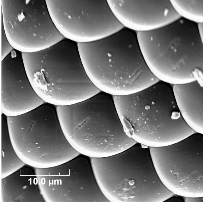 This image shows an SEM image of a house fly's compound eye. Some of the lenses are scratched or have embedded particles on them. This fly died of natural causes and was carbon coated and imaged. Source: Seth Price
Sample preparation
One limitation of SEM imaging is that samples must be conductive. For metallic samples, this is not a problem, but for polymers, ceramics or biological samples, the samples must be coated with a thin conductive layer. Sputter coating of gold, silver or carbon is one common way of coating samples.
Once the sample is or has been made conductive, it can be placed in the SEM chamber. Then, the chamber must be placed under high vacuum. This is perhaps the most time-consuming step. Some samples must be degassed before being placed in the vacuum chamber to reduce the amount of time required to perform SEM analysis.
SEM procedure
After the chamber is under vacuum a beam of focused electrons is rastered across the sample. As electrons crash into the sample, three products of interest are generated: secondary electrons, backscattered electrons and X-rays. Detectors collect these emissions, which is then converted into human-understandable information.
Topographic data
The secondary electrons are bumped from the surface layer of the sample. Basically, the high-energy electron from the electron beam crashes into electrons on the surface of the sample, blasting electrons out of their orbits. Ridges and high spots tend to allow more electrons to escape, and valleys and low spots allow fewer electrons to escape. Therefore, the detector can be used to map high and low spots, or the topography of the sample.
Topographic data can be used to show fatigue lines (beach marks) in samples that have failed due to repeated, cyclic stresses. They can also be used to examine the morphology of a sample, such as the shape of cells, powders, measure thicknesses of coatings and the texture of surfaces to understand how materials failed in use.
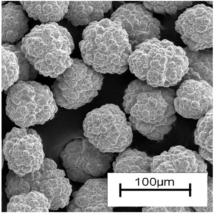 This low resolution image shows a thermal spray powder’s morphology. Round particles, such as these, flow easily through tubes and feeding devices; angular, broken particles do not. Source: Seth Price
Materials characterization with SEM
High energy electrons do not stop by simply contacting the surface of the sample. Many of them dig a little deeper, sending out even more displaced electrons from below the surface as well. When these collisions happen, back-scattered electrons and X-rays are emitted.
Some SEMs are equipped with devices to measure the back-scattered electrons or the x-rays, or both. In machines equipped with these detectors, information about the sample’s composition can be collected. Typically, this involves leaving a sample in the machine for a length of time, while looking for specific elements. Element mapping is a common way to find impurities in materials. Geologists also use this technique to help classify the trace minerals present in rock samples.
This is called electron dispersive X-ray spectroscopy (EDS) though it is sometimes referred to by the brand name of the detector.
Failure analysis
Besides analyzing samples in progress, an SEM can help track down potential problems after an item has failed. Unexpected, catastrophic failures of components can often be traced to materials problems at the microscopic and submicroscopic level.
Using the additional characterization tools such as EDS, the presence of impurities can be detected. Collections of impurities at the grain boundaries of a metal sample can indicate processing issues. Corrosion or corrosion byproducts can be characterized as well.
Topographically, the secondary electrons can show whether a material has failed in a brittle or ductile fashion. A transition between ductile to brittle failure modes can indicate poor heat treating conditions, surface coating issues and other such problems. Beach marks can indicate fatigue failure due to cyclic loading.
Protecting trade secrets
In the microelectronics industry, SEMs are used to collect vital information through different stages of production. The individual wafers and sometimes die level observations are necessary to ensure that CVD coatings are not spalling, to ensure proper etching has occurred and other such metrics.
At this magnification, some of the company’s intellectual property can be easily viewed. To protect the trade secrets of the microelectronic configurations, chip designers can implement metric markers, such as holes, parallel lines or other such markings. Instead of the SEM technician viewing potentially thousands of copies of the intellectual property each shift, they instead can view and measure the markers that will represent the features of interest. Then, if more detailed measurements are required, that particular wafer can be examined by a design or process engineer.
Final thoughts
SEM technology and its applications are constantly improving. Perhaps the biggest areas of development are higher resolution beams, better vacuum technology and the use of artificial intelligence (AI) to perform image analysis functions. Because the biggest time sink for SEM analysis is in the vacuum system, this is an area of major development, though the analysis itself can take a lot of time as well.
For the semiconductor industry, smarter image analysis means more chips can be examined quickly. Chips that have poor metrics can be flagged for more detailed inspection by a technician or engineer trained in the particular process that is of concern. This provides larger data sets, as more chips can be checked, without requiring plant personnel to view every single one.