Flat Gallium is Newest 2D Material
S. Himmelstein | March 13, 2018A method to engineer atomically flat gallium shows promise for nanoscale electronics. The 2D gallenene 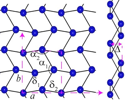 Gallenene structure after exfoliation from bulk gallium. Source: The Ajayan Research Group/Rice Universitydeveloped by researchers from Rice University and the Indian Institute of Science, Bangalore, is a thin film of conductive material that is to gallium what graphene is to carbon.
Extracted into a 2D form, the material appears to have an affinity for binding with semiconductors such as silicon and could make an efficient metal contact in 2D electronic devices.
Gallium has a low melting point and unlike graphene and many other 2D structures, it cannot yet be grown with vapor phase deposition methods. The metal also has a tendency to oxidize quickly, and while early samples of graphene were removed from graphite with adhesive tape, the bonds between gallium layers are too strong for such a simple approach.
The researchers relied on heat instead of force, working their way down from bulk gallium by heating it to 29.7 degrees Celsius (85 degrees Fahrenheit), just below the element’s melting point. That was sufficient to drip gallium onto a glass slide, and a flat piece of silicon dioxide was pressed on top as each drop began to cool so as to lift just a few flat layers of gallenene.
Gallenene was successfully exfoliated onto other substrates, including gallium nitride, gallium arsenide, silicone and nickel. This allowed confirmation that particular gallenene-substrate combinations have different electronic properties and indicated that these properties can be tuned for specific applications.
The material’s plasmonic and other properties are now being investigated.
The research is published in Science Advances.