Graphene “Copy Machine” Creates Cheap Semiconductor Wafers
S. Himmelstein | April 24, 2017The overall cost of wafer manufacturing is poised to decline with new graphene-based technology from MIT. The development supports the fabrication of devices from more exotic, higher-performing semiconductor materials than conventional silicon.
Graphene functions as a sort of “copy machine” to transfer intricate crystalline patterns from an underlying semiconductor wafer to a top layer of identical material.
After placing single sheets of graphene onto an expensive wafer, the researchers grew semiconducting material over the graphene layer. Graphene is thin enough to appear electrically invisible, allowing the top layer to see through the graphene to the underlying crystalline wafer, imprinting its patterns without being influenced by the graphene.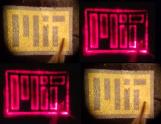 This image shows LEDs grown on graphene, then peeled. Source: MIT
The slippery nature of graphene prevents it from sticking to other materials easily, enabling the engineers to simply peel the top semiconducting layer from the wafer after its structures have been imprinted. In conventional semiconductor manufacturing, once the wafer's crystalline pattern is transferred, it is so strongly bonded to the semiconductor that it is almost impossible to separate without damaging both layers.
Manufacturers can now use graphene as an intermediate layer, allowing them to copy and paste the wafer, separate a copied film from the wafer, and reuse it many times over. The technique saves on the cost of wafers and opens opportunities for exploring more exotic semiconductor materials.
This “remote epitaxy” approach proved successful in copying and peeling off layers of semiconductors from the same semiconductor wafers. The researchers successfully applied the technique to exotic wafer and semiconducting materials, including indium phosphide, gallium arsenide, and gallium phosphide — materials that are 50 to 100 times more expensive than silicon.
The graphene-based peel-off technique may also advance the field of flexible electronics. In general, wafers are very rigid, making the devices they fuse to similarly inflexible. Now semiconductor devices such as LEDs and solar cells can be made to bend and twist. The researchers demonstrated this possibility by fabricating a flexible LED display, patterned in the MIT logo.
The next goal is to design a reusable “mother wafer” with regions made from different exotic materials. Multifunctional, high-performance devices based on graphene as an intermediary will be investigated, along with the potential for mixing and matching various semiconductors and stacking them up as a multimaterial structure.


This is no minor feat in itself. If it speeds up wafer fab, and simultaneously improves reliability, then why not?