Measuring Mechanical Properties of 2D Monolayer Materials Achieved
Siobhan Treacy | January 17, 2018The thinnest materials that can currently be produced — known as two-dimensional materials — have the thickness of a single atom. They exhibit properties that are very different compared to their bulkier three-dimensional counterparts. Until recently, 2D materials were produced and manipulated as films on the surface of some suitable 3D substrates.
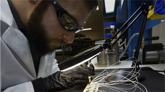
 Working in collaboration with a team from the Leibniz Institute for New Materials, a group of physicists at Saarland University, led by Professor Uwe Hartmann (photo), has for the first time succeeded in characterizing the mechanical properties of free-standing single-atom-thick membranes of graphene. Source: dasbilderwerk
In collaboration with a team from the Leibniz Institute for New Materials, a group of physicists at Saarland University, led by Professor Uwe Hartmann, have succeeded in characterizing the mechanical properties of free-standing single-atom-thick membranes of graphene. The measurements were performed using scanning tunneling microscopy (STM).
Physicists have only known about two-dimensional materials for a few years. In 2010, the scientists André Geim and Konstantin Novoselov were awarded the Noble Prize in Physics for their research work on the material graphene — a two-dimensional allotrope of pure carbon.
After that discovery, a number of other 2D materials made from silicon or germanium were produced or characterized.
"The special feature of these materials is that they are only one atom thick — they are practically all surface," explains Professor Uwe Hartmann, an experimental physicist at Saarland University.
As a result, they possess physical properties that are wholly different to their more conventional three-dimensional relatives.
"The electronic properties of some configurations of graphene are spectacular. The electrons in the interior of the material are relativistic, i.e. they obey the laws of relativity theory, which is certainly not the case for electrons in conventional materials. This suggests a number of interesting advantages for electronic components manufactured from two-dimensional materials," said Hartmann.
The mechanical properties of these 2D materials are also unique. According to Hartmann: "Some configurations of these two-dimensional materials exhibit a degree of mechanical stability that is — relative to the thickness of the material — far greater than that seen in the most stable three-dimensional materials."
In order to exploit the potential, the EU established the Graphene Flagship Project in 2013. It is the EU’s largest research initiative.
Information on the mechanical properties of the novel materials has been derived from simulations.
"Up until now, working with two-dimensional materials has meant working with ultrathin films on the surface of a suitable three-dimensional substrate. As a result, the properties of the overall system are inevitably determined by the three-dimensional material," explains Hartmann.
Working in collaboration with the Leibniz Institute for New Materials (INM), which is located on the Saarbrücken campus, Hartmann’s research team at the Department of Nanostructure Research and Nanotechnology succeeded, for the first time, indirectly measuring the mechanical properties of free-standing single-atom layer membrane of the carbon allotrope graphene.
"We are now in a position to directly compare the data from model calculations with our experimental findings. In addition, we can now measure how different defects in the membrane's crystal lattice affect its mechanical properties," said Hartmann.
The two-dimensional materials hold significant promise of innovative developments in a variety of technological sectors from sensors and actuators to filter systems and fuel cells. The results and methods developed are of major interest for many fields of research.
Scientists in Saarbrücken used a graphene monolayer that was supported on the substrate with a regular array of circular holes. Hartmann explains, "The holes had a diameter of about one micrometer. Using a scanning tunneling microscope (STM) we were able to analyze the free-standing membrane above the holes with atomic precision. When an electrical voltage is applied between the tip of the STM and the single-atom-thick membrane of graphene, electrical current flows."
This current, called the "tunneling current" is sensitive to the distance between the microscope tip and the membrane sample and to the electron distribution in the graphene film. This effect is used to make individual atoms visible to the team. But they also use a different effect. When a voltage is applied between the tip of the STM and the sample, a force acts on the free-standing graphene membrane so it bulges at the tip.
"As the tip is withdrawn, the atomically thin monolayer bulges even more, as it is effectively being lifted up by atomically precise tweezers. Measuring the membrane deflection as a function of the electrostatic pulling force generated by the STM yields a stress-strain diagram that provides us with the key mechanical properties of the graphene membrane," explains Hartmann.
"By recording these experimental stress-strain diagrams, we have been able to directly verify the extraordinary mechanical properties that have been presumed up until now for these materials. And we were able to do this using forces of the order of a billionth of a Newton — far, far smaller than any force used in a conventional mechanical measurement," said Hartmann.
The researchers were also able to show that when a force was applied to a free-standing membrane of graphene, the membrane did not behave like the smooth skin of a kettledrum but looked much more like the rippled surface of a lake. The membranes exhibit a range of wavelike motions and they respond to any external disturbance by generating new ripples in the membrane's surface.
The paper on this research was published in the journal Nanoscale.