Ensuring thermomechanical and electrochemical reliability in AI data centers
July 30, 2026Data centers' energy demands are growing rapidly. According to the International Energy Agency (IEA), electricity consumption from data centers is expected to grow at roughly 15% per year, shifting from 1.5% to 3% of global power demand by 2026. A growing share of this demand stems from AI workloads — including training and inference — where power-hungry processors containing hundreds of billions of transistors operate at scale. Workloads once confined to traditional high-performance computing (HPC) environments are now migrating into data centers, prompting facilities worldwide to retrofit, upgrade or build entirely new infrastructure to support AI.
The xPUs driving these workloads — graphics processing units (GPUs), central processing units (CPUs), tensor processing units (TPUs), neural processing units (NPUs) — are experiencing rapid power escalation. High-end processors that once drew 800 W are now pushing into multi-kilowatt territory. The challenge compounds at the voltage level: as core voltages drop below 1 V, current consumption surges, with 2,000 A and beyond rapidly becoming the norm. High-density racks must simultaneously support multiple 1 U and 2 U server chassis, each housing motherboards with ultra-fine features, often using TSMC’s CoWoS packaging, and an increasing density of semiconductor components. These systems must be effectively powered and cooled to manage the mechanical, electrical and thermal stresses of high-current transients. Underpinning all of this is an uncompromising uptime requirement: in AI factories operating at this scale, failure is simply not an option.
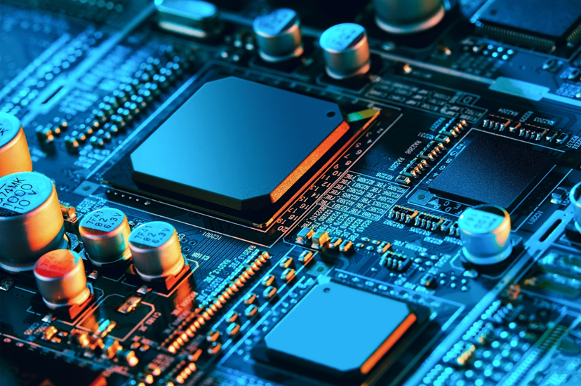 Figure 1. The functional demands of HPC applications and data centers have created a plethora of challenges for assemblers seeking to ensure the reliability of next-generation packages. Source: raigvi/Shutterstock
From the processor's power delivery network (PDN) to voltage regulation, packaging is a critical design challenge for AI with considerations spanning thermomechanical reliability, electrochemical integrity and assembly yield. As HPC packages grow larger and move through increasingly demanding reflow profiles, the margin for error narrows. This paper examines how MacDermid Alpha Electronics Solutions has developed an integrated materials strategy — spanning solder paste, alloy design, flux chemistry, mechanical spacers and polymer reinforcements — to address the specific pain points data center original equipment manufacturers (OEM) face in assembling and ensuring the reliability of next-generation HPC packages.
Warpage-induced defects
The combination of large CoWoS package geometries (up to 200 mm × 200 mm) and smaller pitches (tightening to 0.4 mm to 0.5 mm) increases the risk of warpage due to the non-wet opens (NWOs), head-in-pillow (HiP) failures and bridging failures (Figure 2).
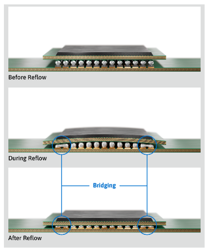 Figure 2. Large form factor packages warpage demonstrating induced bridging failures. Source: MacDermid Alpha
HiP is a solder joint defect whereby the solder joint is thin in the middle with the bulk of solder deposited on the perimeter. As a result of heating-induced warpage and the solder spheres' bulk being unable to come together to form a single mass, a solder joint is produced with a divot in its center. In cross-sectional view, this has the appearance of a head in a soft pillow. This defect can lead to a connection that has intermittent electrical integrity due to a poor mechanical connection with the board.
Similar to HiP, another solder joint defect is NWO. In this case, the solder paste deposited on the pad adheres to the component side, ultimately preventing the formation of an intermetallic connection between the solder and the substrate. This defect is often caused by oxidation on the board. As with HiP defects, NWO defects often result in an intermittent electrical connection.
Bridging occurs when an unintended solder connection forms between two adjacent pads, pins or traces on the PCB, creating an unintended electrical path. The risk of this defect increases due to warping from bending or twisting of the board during reflow, and from the use of excess solder paste, which is often required in large HPC packages. Aberrant conduction due to bridging can result in electrical shorts and impaired circuit functionality.
Both head‑in‑pillow (HiP) and non‑wet‑open (NWO) defects have become more prevalent following the transition to lead‑free soldering, largely due to higher reflow temperatures, increased oxidation and reduced process margins associated with lead‑free materials. Factors increasing their likelihood include oxidation of solder materials, inappropriate reflow issues and insufficient solder paste. Furthermore, the need for ultrafine features required in next-generation applications increases the risk of bridging failures. The mechanical stress of warpage has a particular effect on the risk of HiP and bridging. Significantly, all three of these defects are not easily identified during assembly or in functional testing and may only be detected following a failure during usage.
A complex warpage and ultra-fine feature problem with no room for error
AI processor packages — like TSMC’s CoWoS or Intel’s EMIB — often develop unique, asymmetric warpage signatures during reflow due to die placement geometry and thermal incursion during solder melt.
These warpage-induced defects are not only detrimental to thermomechanical reliability but also to first-pass yield. Increasing defect-per-million levels places additional strain on the assembly process, as assemblers face a zero-rework mandate, meaning defects must be addressed at the start. And with packages ranging from $10,000 to $50,000 per unit, the economics of data center assembly can quickly become a major obstacle to data center success.
As the size and mass of xPU processor packages and the PCBs to which they are attached increase, they often require longer duration reflow profiles. The increased duration is to ensure the variation in temperatures across the assembly is reduced to an acceptable level while also ensuring the entire assembly reaches the proper temperature for soldering. The profile duration may require as much as 11 minutes or more where typical reflow profiles are generally six minutes or shorter in duration. The extended duration increases the time the assembly is experiencing dissimilar warpage, which can lead to an increase in warpage related HiP and NWO defects and increased cumulative thermal stress on the assembly.
Electrochemical reliability: Solder pastes for ultra-fine features
A significant challenge in the processing of these larger packages is the need for ultra-high-density interconnect, in which more semiconductor content is packed into the same board area, while maintaining a high degree of electrochemical reliability. The current IPC standard for electrochemical reliability testing is a spacing of 500 µm. However, the need for increased functionality with no additional board space for next-generation applications requires spacing as low as 100 µm while maintaining electrochemical reliability.
With these ultra-fine features, maintaining electrochemical reliability can be a competing goal, as closer conductor placement increases the risk of electrochemical ion migration from anode to cathode, resulting in dendritic growth between components and increasing the risk of shorts in the circuit.
The tightening of component spacing below IPC electrochemical reliability standards is driving the development and use of high-quality solder pastes that can support ultra-fine features, maintain a constant print volume with area ratios as low as 0.60, deliver high transfer efficiencies and feature apertures below 200 µm (Figure 3). For the maintenance of consistent print volume under variable conditions (e.g., humidity), formulations must be validated according to stringent surface insulation resistance (SIR) profiles, maintaining comb spacings as low as 100 µm to 200 µm, without compromising electrochemical reliability.
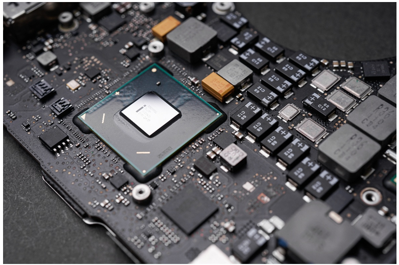 Figure 3. To mitigate the risk of dendritic growth in AI processor boards with ultra-fine features, specialized solder pastes must meet challenging SiR profiles. Source: Capix Denan/Shutterstock
The combination of thermomechanical solutions, such as copper spacers and specialized solder pastes for ultra-fine features, provides a practical approach to controlling warpage during reflow, while next-generation paste chemistries reduce the incidence of electrochemical failures. Solder paste chemistries can be explored to further reduce warpage-induced defects while also supporting ultra-fine features.
Integrated solutions that address all potential failure mechanisms — considering electrical, chemical, thermal and mechanical modalities — are critical to effectively assembling cutting-edge processor solutions that push the envelope on multiple fronts.
Compatibility is also a consideration for assemblers. Many will use high-reliability silver, tin and copper (SAC)-based alloys (e.g., SAC305, SACX and Innolot) that are developed specifically for harsh-environment applications. If OEMs or original design manufacturers (ODM) are already using these alloys, then the solder paste chemistry must demonstrate compatibility with their distinct melting behavior and microstructural properties.
Thermomechanical reliability: High-reliability alloys
These high-reliability alloys are defined by their resistance to creep, or the propagation of deformation within the grain structure of the solder, which causes it to coarsen and thus weaken, until a crack forms and progresses through the bulk of the joint. This is a problem in HPC and data center environments where solder joints can experience significant thermomechanical strain during intensive AI workloads, with transients of up to 1,000 A/µs. Joule heating, a process by which heat is produced by resistance as high-amplitude current passes through the system, can cause solder joint failure through creep and cracking over thousands of transient events.
These SAC-based alloys often add dopants and additional alloying elements to ensure a finer grain structure that can withstand creep at higher temperatures. The finer the grain structure, the more grain boundaries and the greater the crack propagation resistance.
Extended in-use life through polymer reinforcements
Since these boards meet mission-critical uptime requirements, polymer reinforcements can extend in-use life, providing an elevated level of reliability by redistributing any thermomechanical stress during thermal cycling and power transients.
Other common reinforcement strategies, like underfills, edge-bonds and corner-bonds, mechanically support key solder joints. Underfills, for example, fill the area beneath the package, fully encapsulating the solder balls with a polymer that exhibits a high glass transition temperature (Tg) and a low coefficient of thermal expansion (CTE). Edge-bonds and corner-bonds provide more targeted support for solder joints, improving long-term in-use life.
Using materials with well-matched CTEs and an optimal Tg is critical to matching package and substrate behavior — heating a material above its Tg will cause it to soften and increase its CTE, leading to CTE mismatch and downstream reliability issues such as solder joint fatigue and creep. Beyond their thermomechanical benefits, these materials must also often consider any additional process complexity and potential warpage interactions.
An integrated solutions partner
The functional demands of HPC applications and data centers have created a plethora of challenges for assemblers seeking to ensure the reliability of next-generation packages. The increasing package size needed to deliver the required functionality has resulted in greater exposure to thermal stress during assembly due to extended reflow profiles, increasing the risk of warpage and subsequent solder defects.
Alongside this, the ultra-fine density of component placement within these packages and the increased power they process create further challenges in maintaining thermomechanical and electromechanical reliability. The high cost of these processors, with no option for rework, provides little margin for error in assembly.
These complex problems require complex solutions at the assembly level, and MacDermid Alpha Electronics Solutions is approaching this with an integrated solutions strategy. This integrated strategy combines various aspects during assembly, including mechanical support for the board, high-quality solder pastes and flux chemistries and polymer reinforcements, providing a multifaceted approach that looks to the future of next-generation package assembly.
Looking ahead, MacDermid Alpha’s ALPHA® HiTech® roadmap is designed to help manufacturers stay ahead of next-generation assembly realities, from rising power density and faster computing to smaller form factors and longer required service life, where materials choices increasingly determine real-world performance.
By continuing to engineer soldering, reinforcement polymers and protection technologies as a coordinated materials system, MacDermid Alpha enables more predictable outcomes at scale -balancing thermal performance, mechanical integrity and manufacturability from design intent through volume production.
The ALPHA HiTech platform emphasizes integrated material solutions – including solder technologies, reinforcement materials, underfills, edgebonds and encapsulants that improve board-level durability and reliability while supporting the process efficiency and compatibility needed for advanced package assembly.
And as sustainability expectations tighten, MacDermid Alpha is pairing reliability advances with a clear commitment to solutions that minimize waste and reduce energy consumption, helping customers meet performance targets without losing sight of environmental objectives.
Data center OEMs and ODMs facing assembly and reliability challenges with next-generation HPC packages can work directly with MacDermid Alpha Electronics Solutions' engineering team to identify the right combination of materials for their specific package architecture and process requirements. By partnering early in the design and assembly process, manufacturers and designers can better understand how material selection influences yield, reliability and long-term performance.