SubFab: 5 ways chipmakers could fix their hidden infrastructure
Peter Brown | October 23, 2026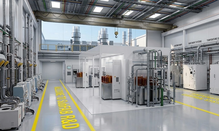 A rendering of the first dedicated semiconductor SubFab R&D facility. Source: ISRL USA/AIIP
For decades in the semiconductor industry, the inside of a process chamber of a fab has gotten all the attention, because that is where the yield, transistor performance and competitive advantage are created. Downstream, where the leftover chemistry goes, the unglamorous, essential support systems known as the SubFab have largely been overlooked.
Some of the most dangerous chemistry, highest energy consumption and largest environmental impact in semiconductor manufacturing happens downstream from the process chamber inside the SubFab, the infrastructure layer beneath the cleanroom. For example, in advanced 3D NAND manufacturing, dry etch can account for roughly half of manufacturing emissions due to the combined impact of plasma systems, vacuum infrastructure, chillers and gas abatement, according to data from market research firm TechInsights.
Yet firms tend to pass it off as utilities rather than a scientific discipline, Scott Balaguer, CEO of International SubFab Research Labs (ISRL USA), told Electronics360.
“That is not sustainable engineering, that is containment.” Balaguer said. “The industry did not ignore the SubFab because it was unimportant. It ignored it because it was fragmented.”
But this may be changing.
In April 2026, ISRL USA and AI Infrastructure Partners (AIIP) said they will collaborate to build what they claim is the first purpose-built SubFab R&D facility. This will bring together an ecosystem of semiconductor manufacturing vendors, materials companies and research institutions to replicate high-volume manufacturing conditions. The R&D facility will research sustainability challenges in the SubFab and potentially develop standards and best practices for sustainability.
Why focus on it now?
These sustainability challenges have grown due to the combination of the demand from AI infrastructure and advanced-node manufacturing for:
- High-bandwidth memory
- Advanced packaging
- AI accelerator production
- Leading-edge logic
“In advanced manufacturing, many of these [SubFab] systems operate continuously, even when tools are idle, resulting in a significant operational footprint,” said Stephen Russell, senior technical fellow for sustainability at TechInsights. “Sustainability has shifted from being primarily a reporting exercise to becoming a large-scale operational engineering challenge.”
And the industry now recognizes that long-term sustainability improvements will depend heavily on infrastructure optimization, not just improvements inside the process chamber itself, Russell added.
“This is no longer ‘green marketing,’” Balaguer said. “This is core manufacturing optimization. And frankly, the industry also realized that many net-zero commitments cannot be achieved without addressing the SubFab layer directly.”
TechInsights forecasts increasing levels of scrutiny in the chipmaking sector to be focused on SubFab infrastructure over the next several years.
A competitive advantage
That includes potentially becoming so operationally sophisticated that the SubFab becomes a competitive differentiator for fabs that make it a priority as they manage energy, water and emissions to gain both sustainability and cost advantages, TechInsights’ Russell said.
Additionally, TechInsights expects growing attention in the SubFab regarding:
- Fluorinated gas accounting
- Integrated abatement approaches
- Increased water recycling
- Stronger pressure for Scope 3 carbon emissions transparency
- System-level energy optimization across fabs and infrastructure
“We also expect much greater demand for granular process-level and tool-level sustainability data,” Russell said. “Historically, semiconductor sustainability discussions relied heavily on facility averages, but the industry is increasingly moving toward hotspot analysis that identifies emissions-intensive process modules such as lithography, etch, deposition, and supporting infrastructure.”
A potential SubFab future
Balaguer said that the SubFab that exists in five years will look much less like a utility corridor and more like an intelligent process ecosystem. This includes:
- AI-based predictive control of pumps and abatement systems
- Real-time chemistry monitoring
- Reductions in unnecessary nitrogen purges
- Modular infrastructure designed for rapid process transitions
- Better heat recovery and energy optimization
Some of this could come from tying SubFab equipment to what the other parts of the fab are doing. John Behnke, GM of smart manufacturing at Inficon, described two levels of this to Globalspec. At level one control, equipment responds in real time, so abatement runs only when a tool is actually using process gas. At level two, Behnke said, the system also looks ahead to the factory production schedule. For example, if an area of a fab will be light on material for the next few days, the abatement serving that idea could be idled instead of kept at full readiness.
This is where a big opportunity potentially resides for fab builders to save on energy and power consumption as well as environmental impacts, Behnke added.
“Most importantly, the SubFab will become visible,” Balaguer said. “Today, many fabs operate the SubFab almost blindly. In the future, operators will understand downstream chemistry with the same sophistication they currently apply inside the chamber. That is the transformation.”
Behnke agreed that the industry has "largely ignored the darkness in the SubFab" due to the chipmakers focused more on enabling the products. However, that is starting to change, he said.
Future collaborations
Due to the growing pressure for sustainability data across the chip supply chain, industry collaboration might be the way this future SubFab becomes a reality. The SubFab R&D facility would help in creating methodologies and verification for these processes, Russell said.
“No single company can independently solve fluorinated gas management, water stress, or grid-capacity constraints across the entire semiconductor supply chain,” Russell said. “Carbon data is increasingly becoming part of supplier qualification and procurement decisions.”
Collaboration between supply chain partners is more common than people think as the ecosystem already works together with frameworks, supplier ecosystem and shared sustainability targets, he added. Through the SubFab R&D facility, similar standards and best practices are likely to emerge.
Conclusion
"In many ways, the SubFab is becoming the hidden engine room of semiconductor sustainability," Russell said.
Balaguer said the industry is already moving, with operational and monitoring improvements able to scale within two to three years and broader infrastructure redesigns likely taking five to 10.
"The conversation changed from 'Should we address the SubFab?' to 'How fast can we do it without slowing innovation?’” Balaguer said.