
A Concise Chronicle of Thin-Film Maturation
February 28, 2018Sponsored content
The use of thin films to enhance the physical and chemical properties of materials is a common practice with diverse applications, from coating architectural glass to manipulate light and heat transmission, to the design of absorber layers for solar cells to magnetic thin films for electronic data storage. The technology may be considered largely a processing product of the 20th century, but its roots extend much further in the past.
As far back as ancient Egypt, the first documented thin films were gold layers produced chemo-mechanically by Egyptian artisans about 5,000 years ago. The decorative films were gilded on copper and bronze jewelry, statues and other objects.
There is also evidence of an autocatalytic solution-growth technique involving oxidation/reduction reactions developed by Peruvian Indians at around 100 BC. The process used locally available minerals to deposit gold and silver films on copper and bronze artifacts. This scheme is still in use today, although conducted more efficiently as electroless plating.
 Figure 1. Diagram of a Gaede pump. The advent of modern vacuum technology for thin-film deposition began with the design of the first high-vacuum pump by Wolfgang Gaede, who filed a German patent application in 1907. Two years later, Robert Wichard Pohl used this technique to produce thin silver films for Fabry-Perot applications that control and measure the wavelengths of light.
Alexander Smakula was a Ukrainian physicist known for the invention of anti-reflective lens coatings based on optical interference. While employed at Carl Zeiss AG in Jena, Germany, during the 1930s, he observed that when light enters or leaves a lens, a certain percentage of the light is reflected from the boundaries. To counter this loss, Smakula covered lens’ surfaces with extremely thin layers of special materials to reduce reflections and improve light transmission. Such anti-reflective coatings are now applied to optics for cameras, solar panels and many other products and instruments.
Sputtering is the fastest growing of the vapor-phase deposition techniques, as it is relatively insensitive to deposition temperature and is easily controllable. In 1852, William Robert Grove, a Welsh lawyer and physicist, published the earliest recorded description of sputter deposition and ion-etching experiments.
Between the mid-1970s and early 1990s, reactive sputtering emerged as a major thin-film synthesis technique for both research and industrial applications. This interval is marked by the development of high-rate reactive sputtering, the availability of pulsed-DC and mid-frequency power supplies and the evolution of atomic-scale models for controlling the complex processes inherent in reactive sputtering.
Other thin-film technologies evolved rapidly in the last few decades, including the development of about a dozen ion-based coating processes. Cathodic arc deposition was established as an energetic condensation process, first in the former Soviet Union in the 1970s and later in the 1980s in the Western Hemisphere.
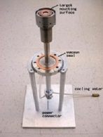 Figure 2. A magnetron sputter gun showing the target-mounting surface, the vacuum feedthrough, the power connector and the water lines. Source: Chaiken / CC BY-SA 3.0Two new forms of magnetron sputtering were created during the 1990s, both with the goal of efficiently ionizing sputter-ejected metal atoms. The first ionized-magnetron sputter deposition was developed in the early 1990s by IBM researchers to improve coating uniformity. High-power impulse magnetron sputtering was also advanced around this time, which entails applying high-power pulses to the target to produce ultra-dense plasmas with electron concentrations two to four orders of magnitude higher than achieved with standard DC magnetrons.
Thin-film deposition technology is now capable of depositing layers of metals and other materials that are extremely thin and measured in mere nanometers. Thin-film manufacturing techniques are contributing to the first generation of true nanotechnologies, just as they have contributed to cutting-edge technology for over a century.
Cascade Optical Corporation is a manufacturer  of custom vacuum-deposited thin-film coatings with more than 40 years of specializing in ion-assisted deposition, low-temperature, low-stress coatings designed for laser crystals, fiber optics plastic fibers and other delicate substrates. With our specialized techniques, we are able to generate coatings with greater packing densities to handle very high laser damage thresholds. Our vast research and design and innovative coating techniques will work for a wide diversification in the Electro-Optic community. Cascade is continuously upgrading our technologies with the most modern and up-to-date equipment in order to keep pace with industry. And, oftentimes, surpassing the most crucial standards in the market. We provide high-quality, quick lead times and the best pricing to help our customers meet their goals.
For more information, visit http://www.globalspec.com/supplier/Services/CascadeOptical.