Processes Enabling Nanomanufacturing
Gary Kardys | June 09, 2017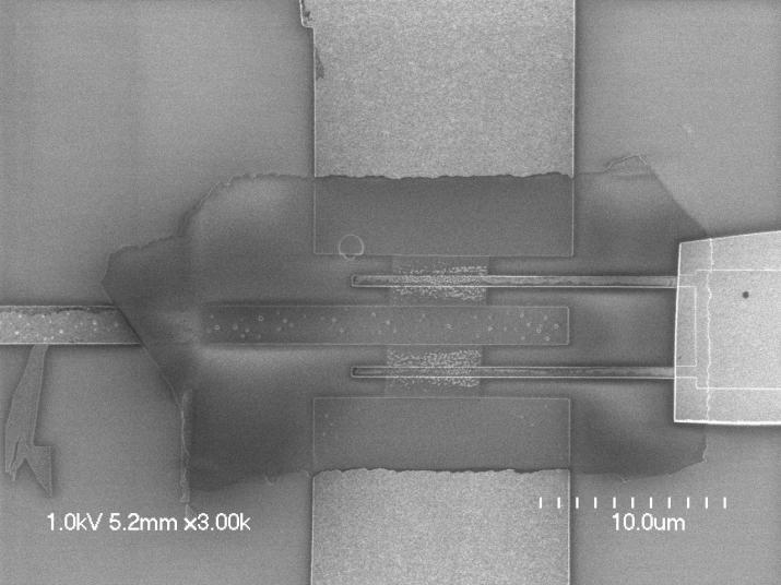 Figure 1 - Transistor with 1 atom thick graphene. A high resolution image of a graphene transistor with a sheet of carbon only one atom thick. This high speed electronic device was created using nanoscale processes, and may one day be used for better computer chips. (Courtesy of James Yardley, Columbia University Nanocenter, an NNI-sponsored NSEC)
The video provides a virtual tour and overview of the CNST Nanofab at the Center for Nanoscale Science and Technology (CNST) on the National Institute of Science and Technology (NIST) campus in Gaithersburg, Maryland. The NanoFab has over 100 commercial process tools within an advanced class 100 cleanroom laboratory space. The tools enable researchers from industry, government and academia to develop and evaluate new nanotechnology processes and advance the field of nanoelectronics and nanotechnology.
Nanomanufacturing engineers have many different processes available to fabricate nanomaterials, nanodevices and other nanotechnology products depending on the specific nanotechnology product being manufactured. Broadly speaking, the two major approaches are top-down and bottom-up nanomanufacturing. Bottom-up nanomanufacturing builds products from atomic- and molecular-scale components using nanofabrication processes such as thin film deposition and lithography processes. Building something from atom or molecules can be an extremely slow process. Nanoscale 3D printing and self-assembly processes and are newer bottom-up processes under development. Powder and particle fabrication methods enable the top-down approach. In some applications, a combination of top-down and bottom-up processes to produce certain nanoscale or nanostructured products might be the appropriate choice.
Nanofabrication Processes
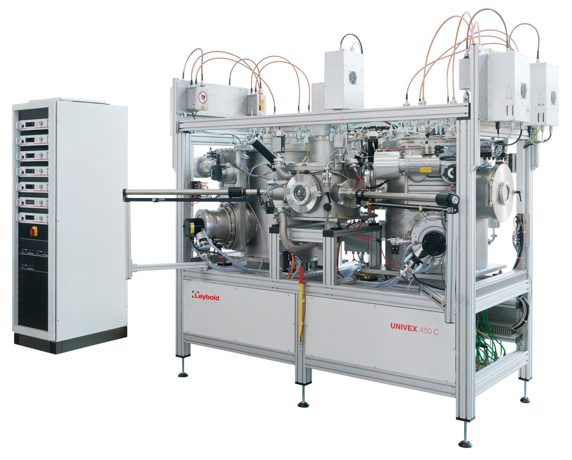 Figure 2 - UNIVEX thin film depostion system cluster tool automates sequence of several types of PVD coating processes for research, pilot and production. (Courtesy: Leybold USA Inc.)Nanofabrication processes are used to create advanced nanoelectronic and nanophotonic devices on silicon and other semiconductor substrates. Chemical vapor deposition (CVD), physical vapor deposition (PVD) processes and other thin film deposition processes are commonly used to produce coating or layers with nanoscale thickness. Advanced lithography and etching methods pattern the deposited films into nanoscale interconnects, insulators, nanotransistors, nanodiodes and other nanosemiconductor devices with nanometer critical dimensions.
Chemical vapor deposition (CVD) reacts two or more component vapors or gases to form and deposit specific compound and materials. Molecular beam epitaxy deposits monocrystalline thin films. Atomic layer epitaxy enables the deposition of single-atom thick layers on substrates. Glancing angle deposition (GLAD) processes can produce nanorod structures directly on a surface. GLAD might be a more viable technique compared to fabricating CNTs or other nanorod particles and then placing them on a surface in an ordered fashion through self-assembly. Electrodepostion or nanoplating is also used to deposit very thin metal films. Many new and evolving thin film deposition processes are under development for nanomanufacturing and nanoelectronics fabrication.
While thin film deposition processes produce a coating or layer with nanoscale dimensions, nanoscale lithography processes allow nanoengineers to control geometry on the third dimension to produce nanoscale devices. Photolithography technologies have a long history in microelectronic device fabrication. In the photolithography process, a photoresist film is deposited over the thin film to be etched, typically using a spin coater. A mask with the circuit pattern is used to expose only certain areas of the photoresist to UV light. A developer is applied and the photoresist is selectively removed. An etching step removes the thin film in regions not protected by the remaining photoresist. Extreme or deep UV lithography uses smaller wavelengths to provide finer resolution compared to conventional photolithography.
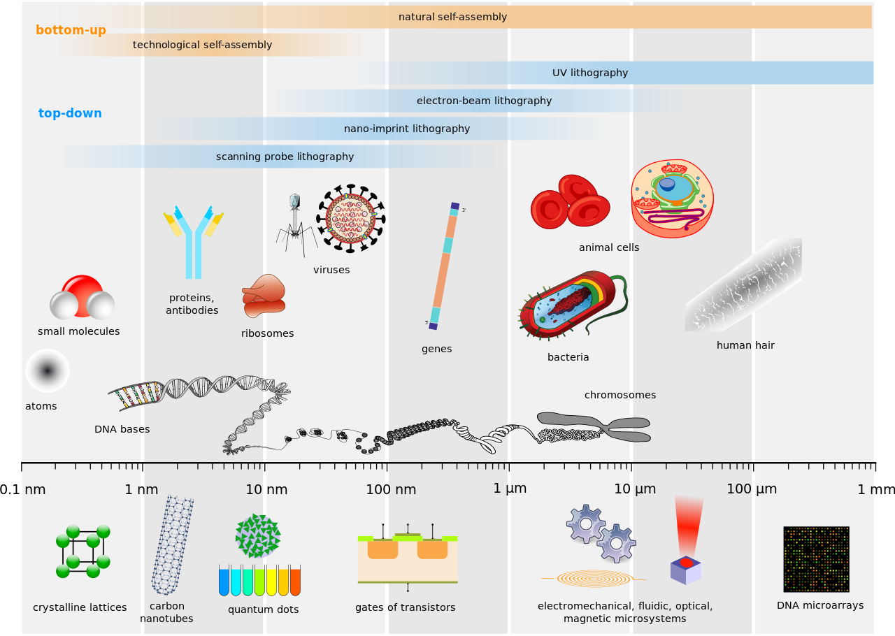 Figure 3 - Biological and nanotechnology scales compared. (Courtesy Wikipedia)
Newer lithography or nanoscale 3D printing processes such as dip pen lithography and nanoimprint lithography are under development to enable even greater resolution and reduction in device-critical dimensions. In the nanoprinting process, the probe of an atomic force microscope is "dipped" into a chemical fluid and then used to "write" on a surface. Nanoimprint lithography uses nanopatterned template (mold or stamp) to "print" or stamp pattern at the nanoscale. The resin is coated on the UV transparent mold, which is pressed against the wafer and cured with UV light .
In nature, biological processes build bone and organs through self-assembly via directions from DNA. Nanoscientists and nanoengineers are trying to develop self-assembled nanostructures using scaffolds, weak bonding, microrobots and biomimicry methods to create ordered nanostructures. Processes for self-assembly and self-organization use nanosized or molecular building blocks that come together to form an ordered nanostructure without outside direction. Scaffolds and weak bonding forces (Van Der Vaals, hydrogen bonding, etc.) are used to guide and control the self-assembled nanostructure.
Nanoparticles and Nanopowder Production Processes
 Figure 4 - Cadmium Selenide quantum dots. (Courtesy Wikipedia)
Nanoparticles and nanomaterials are now indispensable building blocks in catalysts, sensors, photovoltaic devices, photonic devices, displays, capacitors, coatings, nanocomposites, batteries, nanovaccines, nanodrugs, diagnostic imaging tools and a wide variety of industrial applications. In some applications, a powder consisting of nanoparticles, quantum dots, carbon nanotubes, or graphene ribbons or other nanosized particulates are manufactured first. The nanopowder is then compounded, dispersed or self-assembled to produce the finished nanomaterial product. Powders can be produced by several different chemical, mechanical, and thermal processes.
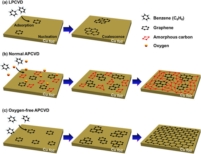 Figure 5 - Chemical vapor deposition synthesis of graphene. (Courtesy Nature, Scientific Reports 5, Article number: 17955 (2015) doi:10.1038/srep17955)Chemical vapor deposition (CVD) and chemical vapor condensation (CVC) processes can also be used to produce nanoparticles and graphene. Precursor gases are reacted and then nanoparticles are deposited or condensed from the reacted vapor. Chemicals solutions are supercritically atomized or spray dried to produce nanoparticles.
Sol-gel, hydrothermal synthesis, solvothermal synthesis and chemical precipitation processes present aqueous or liquid solution routes to nanoparticles and nanostructured materials manufacturing. In the chemical precipitation process, nanoprecipitate particles are formed from a dissolved metal salt solution after pH or chemical changes. Sol-gels are colloidal solution (sol) reacted to form an integrated network (gel). Metal alkoxides precursors are typically the raw materials for sol-gel formation. Sol-gels are dried and fired to make nanostructured ceramics and nanoceramic particles. Hydrothermal and solvothermal syntheses combine some of the aspects of chemical precipitation and sol-gel techniques with thermal and pressure in an autoclave to form nanoparticles and nanostructures. The size, shape distribution, and crystallinity of metaloxide nanoparticles or nanostructures can be precisely controlled with solvothermal synthesis processes. Hydrothermal processes dissolve the metal salt or alkoxides in a water or aqueous solution. Solvothermal processes use a non-aqueous solvent.
 Figure 6 - Flame spray synthesis process for nanoparticle production.
In the spray pyrolysis process, a chemical solution consisting of dissolved metal salt is atomized using gas pressure, ultrasonic nebulization or electrical current and then converted to an oxide or ceramic with a flame, plasma or other heat source.
Mechanical methods used to produce nanopowders include crushing, pulverization, milling and classification. Massive chunks or blocks of metals, ceramics or other materials are first reduced in size with coarse crushing equipment such as a jaw crusher or impact mill. Screening equipment is used to extract the fine portion from the crusher, which is fed to an intermediate mill or pulverizer to produce micron sized powders. An air classifier can cut the fine micron portion from the pulverized powder. The micron 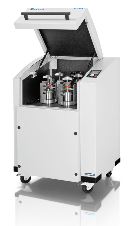 Figure 7 - Retsch Planetary Ball Mill PM 400 for colloidal grinding to submicron particle sizes. (Courtesy Retsch GmbH)powder is placed in a high-energy ball mill or other media mill to further reduce the particle size to the nanoparticle size range. Powder production methods can generate waste or by-products such as micron or macro sized particles, which may or may not have a useful market. The coarser fractions from various process steps can be reprocessed to produce additional nanoparticles depending on the specific material and powder production process. Additional processing or recycling certain materials might alter chemistry (e.g., oxygen levels) outside of allowing specifications.
Melting, evaporation, plasma sputtering, physical vapor deposition (PVD) and other thermal or physical processes can be used to produce nanoparticles. A melt can be atomized to produce fine droplets or micron sized droplets, which cool so rapidly that a nanostructured alloy ceramics results. Explosive melting is used to produce nanoparticles from metals, alloys and conductive ceramics by passing a high current through a wire to rapidly heat, melt and vaporize or explode the material. Plasma and laser sources can be used to rapidly heat materials and produce nanoparticles. In sputtering processes, atoms are knocked off a surface using a plasma source and then deposited onto a surface or condensed into nanoparticles.
Dispersion and Compounding Processes
 Figure 8 - Nanostructured polymer silicate nanocomposite material with improved thermal, mechanical, and barrier properties. (Image courtesy of NASA)Nanocomposites and nanocoatings and are often manufactured using nanoparticles, nanosized powders, carbon nanotubes, or graphene ribbons, which are dispersed in a base resin carrier or matrix. Blenders, industrial mixers, homogenizer, 3 roll mills and ball mills can be used to disperse fine powders in a resin or liquid carrier. Even with the best dispersion equipment, the nanoparticles may require surface treatment to enable wetting by, dispersion in and bonding to the resin matrix. Coatings on nanoparticles can improve stability, chemical functionality, biocompatibility and quantum or nano effects. Wetting and coupling agents are often applied to conventional powders using fluid beds coaters and blenders with integral spray applicators and intensifier bars to prevent agglomeration during the coating process. Nanoparticles might be too small for these conventional methods. Surface treatments are applied to nanoparticle surfaces by suspending the nanoparticles in a solution containing some of the dissolved surface active agent or coating. Nanoparticle agglomerates are broken up using ultrasonicators. The nanoparticles used to identify or treat tumors often require functionalization surface treatments specific to the organ or cancer being targeted. Kardys, et al described such a process to manufacture surface functionalized nanopartilces in the Journal of Nanotechnology article “Amino-Functionalized Silica Nanoparticles: In Vitro Evaluation for Targeted Delivery and Therapy of Pancreatic Cancer”.
Resources
Center for Nanoscale Science and Technology (CNST)
National Nanotechnology Initiative (NNI)
· Bulk Structured Material Synthesis Methods
· Deposition of Nanostructured Films or Nanostructures
· Etching


It seems there is a confusion in the article about the meaning of "bottom up" and "top down" in nanomanufacturing. The article states: "Bottom-up nanomanufacturing builds products from atomic- and molecular-scale components using nanofabrication processes such as thin film deposition and lithography processes." According to Wikipedia (based on the Foresight Institute coining of the terms in 1989): "Bottom-up approaches seek to have smaller (usually molecular) components built up into more complex assemblies, while top-down approaches seek to create nanoscale devices by using larger, externally controlled ones to direct their assembly." Thin film deposition and lithography are clearly "top down" processes, as achieved by large scale machines (deposition equipment and lithography tools). As example of bottom up technique, self assembly of molecules in block copolymers is usually given, pointing to the fact that macroscopic properties (such as large area order) is achieved by the self assembly of polymer chains (i.e. from bottom - up).
All the information about the process of enabling nonmanufacturing is quite update and understandable as well. Thank you for such tremendous update online and really admire this amazing help here. Also, like to share the ivory research reviews updates to everyone for the expert's help.