Team Develops a Plasma-Free Method to Create Semiconductors
Riia O’Donnell | May 25, 2016A team from Pennsylvania State University has developed a technique that they say will allow manufacturers to produce large sheets of thin-film silicon semiconductors at low temperature in simple reactors. The method could produce the materials at a fraction of the cost currently possible.
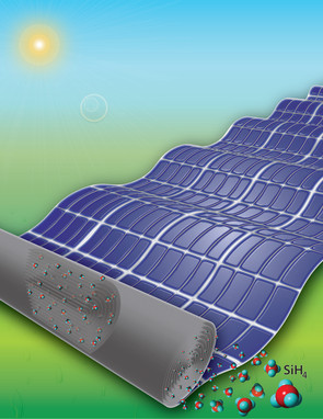 Large-area, thin film semiconducting material. Image source: Penn State UniversityThe method features a high-pressure, plasma-free approach that creates large-area, thin-film semiconductors. By using high-pressure deposition inside rolled-up, flexible substrates the result is a large-area with uniform-thickness, and hydrogenated, amorphous silicon films. The films could be used in a variety of applications, from solar cells to flat panel displays.
Researchers say the traditional, chemical vapor deposition method uses silane to create a chemical reaction. It deposits silicon and hydrogen atoms onto a thin layer, coating a substrate. To achieve this, the chemical reaction must occur at a temperature that is low enough to create a plasma state in reactors that generate the plasma as well as handle the mass volume of gas needed for the process.
The new method allows for low-temperature reactions in a smaller space, with a lower volume of gas. These factors have made it possible for the team to develop semiconductors on multiple stacked surfaces, instead of a single surface, simultaneously.
With further development, they believe the end product could be a rolled-up semiconducting material that could approach or even exceed a square kilometer in size.


