Next generation surface treatment with atmospheric pressure plasma
GlobalSpec News Desk | December 04, 2025The ever-increasing demands of end users on the performance, weight and durability of electronic components are prompting manufacturers to consider new methods and process optimizations. The semiconductor industry, in particular, has traditionally relied on vacuum chambers for plasma surface treatment as a proven method. However, this process has several disadvantages, including high investment costs, limited throughput rates and minimal flexibility for inline production. The increasing miniaturization of components and their growing sensitivity are strengthening manufacturers' desire to explore alternative plasma processes, such as atmospheric pressure plasma. Nevertheless, many electronics industry engineers mistakenly believe that plasma can only exist in a vacuum and that atmospheric pressure plasma damages sensitive surfaces or produces harmful byproducts.
These false assumptions have slowed the adoption of alternatives in the past, despite the growing urgency of the need for faster, safer and more environmentally friendly processes. The future of surface treatment Source: Plasmatreat GmbH requires overcoming these long-held assumptions and trying new solutions. Plasmatreat GmbH is spearheading this change with its atmospheric pressure plasma systems and equipment. This plasma technology, known as Openair-Plasma, operates under atmospheric pressure, can be integrated into manufacturing processes, is suitable for clean rooms and is ideal for processing highly sensitive electronic components. It can efficiently replace costly vacuum chambers and wet chemical cleaning processes. Beyond its technical advantages, the technology offers environmental benefits as well. By replacing chemicals and reducing energy consumption, Openair-Plasma makes production safer and more sustainable, setting a new industry benchmark. Plasma technology has a low carbon footprint, treats surfaces with low-potential plasma and produces no harmful byproducts. Plasmatreat makes this innovative technology available throughout the electronics value chain, including front-end and wafer treatment, artificial intelligence (AI)-controlled packaging, power modules and lead frames.
Surface treatment under atmospheric pressure conditions
Plasmatreat's Openair-Plasma technology provides surface treatment solutions that meet the strict demands of modern manufacturing. This technology uses only compressed air and electricity under atmospheric conditions. Openair-Plasma prepares surfaces for subsequent processes, such as bonding, coating, printing or sealing. Plasma is generated in special nozzles by ionizing clean, compressed air with an electrical discharge. In addition to the plasma nozzles, Plasmatreat's systems consist of a generator and a control unit compatible with Industry 4.0, the Plasma Control Unit (PCU), which enables precise adjustment and verification of process parameters. The power and flow rate are continuously monitored to ensure the plasma process and guarantee the reproducibility of the treatment. Plasma can remove the finest impurities and activate and functionalize surfaces.
Unlike vacuum plasma processes, Openair-Plasma allows for selective, automated and in-line treatment. Manufacturers can now treat only the required areas, reducing chemical and energy consumption and cycle time. These technological capabilities are becoming increasingly important in semiconductor manufacturing and processing.
These advantages have contributed to the widespread adoption of plasma-based processes in the semiconductor industry, including thermal compress bonding, underfill and oxide reduction. Openair-Plasma technology offers a significant cost advantage because only a fraction of the investment costs required for traditional vacuum plasma machines are necessary.
Remove oxides with plasma — for clean surfaces
 Source: Plasmatreat GmbH Uniform surface modification is only one part of the equation. To ensure reliable bonding, manufacturers must also consider oxide layers, which affect adhesive strength and, consequently, the quality of end products. Traditional solutions, such as the use of formic acid, remove these layers; however, they have significant disadvantages, including chemical waste, unstable surfaces, and the need for immediate downstream processing. Plasmatreat's REDOX-Tool offers a groundbreaking alternative. Using in-line plasma technology, the REDOX-Tool removes oxide layers and simultaneously modifies surfaces to achieve perfect bonding properties without the use of aggressive chemicals. The REDOX-Tool uses Openair-Plasma technology in a controlled tunnel system with nitrogen and hydrogen to achieve flux-free bonding and selective oxide reduction without damaging the underlying metal.
This innovation addresses the challenges of the packaging process directly, including miniaturization, reduced bump pitch, and flux residues. It also reduces energy consumption in demanding applications, such as AI devices. By providing a clean, stable surface through an environmentally friendly, in-line process, the REDOX-Tool sets a new standard for quality, efficiency and sustainability in semiconductor and power module manufacturing.
Plasma meets water: HydroPlasma 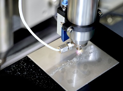 Source: Plasmatreat GmbH
Plasmatreat has expanded its technology beyond standard cleaning to enable environmentally friendly metal oxide reduction. The latest breakthrough is HydroPlasma, which combines the effects of Openair-Plasma with the chemical reactivity of water molecules, offering a new method of surface cleaning. HydroPlasma works by feeding distilled water into the plasma process. The water is ionized, generating highly reactive water molecules. These molecules act like a detergent, cleaning stubborn contaminants from surfaces without the use of aggressive chemicals. A plasma-activated water jet, applied through a specially designed nozzle, effectively removes organic residues, such as oils and fats, as well as inorganic contaminants, such as salts. These contaminants are converted into  Source: Plasmatreat GmbH soluble or gaseous components, thoroughly cleaning surfaces. This makes the technology particularly promising for semiconductor packaging and other industrial applications. With no chemical waste and broad industrial potential, HydroPlasma is a significant advancement in surface treatment technology.
Customized nanocoatings with precise performance
Since nanocoatings play a crucial role in the semiconductor industry, particularly in chip manufacturing, Plasmatreat has developed a solution for the coating sector. The company developed PlasmaPlus technology to enable nanocoatings to be applied under atmospheric conditions. Unlike traditional methods, which use vacuum chambers, the Plasmatreat method applies precursors within atmospheric plasma nozzles to perform chemical vapor deposition directly in open air. Using different precursors allows manufacturers to apply coatings with the desired properties, such as hydrophobicity, hydrophilicity, insulation, moisture barriers, corrosion resistance and improved adhesion. Source: Plasmatreat GmbH
One of the most effective applications of this technology is the selective application of dielectric barrier coatings to electronic components. These coatings provide corrosion protection for batteries, flexible electronics and other sensitive components. The result is a targeted nanocoating for compact, complex devices that support the next generation of technologies, such as augmented and virtual reality systems.
Minimizing ecological footprint while reducing costs at the same time
The advantages of Openair-Plasma and PlasmaPlus applications take manufacturers' perspectives on environmental responsibility to the next level. Plasmatreat combines advanced surface treatment with sustainability, allowing manufacturers to achieve precise surface modification without using harmful chemicals. With global application laboratories, three dedicated R&D centers, and a worldwide network of sales and service offices, Plasmatreat collaborates closely with customers to develop solutions. This partnership model has earned the trust of leading semiconductor manufacturers, especially since Plasmatreat has helped them transition from environmentally harmful cleaning methods, such as formic acid, which dominated semiconductor manufacturing processes for decades. This change reduces environmental impact, as well as operating costs, exhaust gas disposal costs, and waste management costs. At the same time, the technology delivers more reliable and precise surface modification, proving to be a game changer in semiconductor production.
 Source: Plasmatreat GmbH
Conclusion: These advantages have contributed to the widespread adoption of plasma-based processes in semiconductor manufacturing for applications such as thermal compress bonding, underfill and oxide reduction.