Driving sustainability and performance in semiconductor manufacturing: Material solutions for the future
January 31, 2025
Figure 1: Semiconductor manufacturing is a complex process. Source: Hero Design/Adobe
Needless to say, semiconductor manufacturing is a complex process. It encompasses hundreds of precise steps, working with highly sensitive, engineered materials and components, and consumes a vast array of resources. It is supported by lengthy supply chains and the efforts of a highly skilled workforce.
This industry application has become more difficult in recent years due to regulatory and market pressure to increase sustainability efforts. Process and design engineers, procurement teams, quality assurance and sustainability auditors and supply chain personnel all have their work cut out for them when energy enhancements are ever-looming, or when materials like PFAS are scrutinized.
On top of this, key performance parameters for these semiconductors cannot be changed —entire devices and downstream workflows depend on them. Electrical conductivity, thermal management, durability and reliability, among others, are chief performance considerations. Integration into existing or future product designs, as well as their workability within production lines, are equally as important.
These challenges are not insurmountable, as leading innovators continuously look to address them. One promising trend can be seen in the field of integrated materials, where research and development have yielded innovative solutions specifically geared toward enhancing performance, reliability and sustainability for semiconductor manufacturers.
Defining semiconductor sustainability
In the context of electronics, the concept of sustainability can be seen as minimizing environmental and social impacts while still allowing for technological progress. Designing for energy efficiency, promoting recycling, eliminating toxic or unethical materials, and exploring new manufacturing methods are all sustainability strategies that can be found in today’s semiconductor manufacturing landscape. When these strategies succeed in the field, they may be adopted into regulatory or industry standards to encourage wider adoption.
For instance, the American National Standards Institute (ANSI) maintains a range of standards for semiconductor devices that address common industry pain points around sustainability, including hazardous materials. These standards were organized around the guidelines of the International Electrotechnical Commission (IEC) which address design, manufacturing and certification of electrical products and systems.
It is these types of standards that are advising regulatory guidance on PFAS in both North America and Europe. PFAS (Per- and polyfluoroalkyl substances) are a group of synthetic chemicals widely used for their resistance to heat, water and oil. They are found in a variety of products, including non-stick cookware, waterproof fabrics, food packaging and industrial applications. However, PFAS are often referred to as "forever chemicals" because they do not break down easily in the environment and can accumulate in living organisms.
PFAS can be found in various chemicals, equipment and devices used in semiconductor manufacturing, such as photoresist liquids, adhesives, etch chamber gases, high-purity water systems and lithium batteries. Additionally, PFAS can be present in final semiconductor products like microprocessor chip casings, as well as in equipment used to produce components and chemicals essential to semiconductor production.
Concerns over the potential health impacts and environmental persistence of PFAS became publicly established in the late 1990s, prompting the phaseout of one type: perfluorooctane sulfonate (PFOS). After PFOS was phased out, an alternative polymer was introduced in 2004 that used a short-chain PFAS, which meant it would linger for less time in the human body following exposure.
This became the dominant material in the market, but it solved one problem while creating another: The short-chain substances were more environmentally mobile than the materials they replaced. Various scientific studies have concluded that PFAS pollution has no limits —everything from drinking water to food supply chains to consumer and personal products has shown evidence of forever chemical contamination.
The biological repercussions of PFAS are the most serious but do not stand alone. Consumers show strong brand and product preferences toward those that exhibit conscientious sourcing and manufacturing practices. Additionally, the tracking and reporting of continued PFAS use adds another layer of operations and red tape.
This is not to say that the challenge is unresolvable. Wherever possible in the manufacturing process, fabricators are seeking to limit PFAS to applications where no suitable substitute yet exists, which is fostering innovation.
PFAS-free innovative material solutions
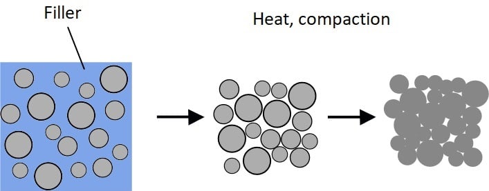 Figure 2. Sintering creates atomic diffusion without the need for a phase change by applying heat and pressure over time. Source: Krb19, BY-SA 4.0
Outside of sustainable solutions through environmental and social impact minimization in semiconductor manufacturing, there is a parallel push for innovation through enhanced methods of production which can intertwine with the latter. Sintering creates atomic diffusion without the need for a phase change by applying heat and pressure over time to a nanoparticle powder. It can be performed with both copper and silver, each of which has been used to replace metallic lead for compliance with the Restriction of Hazardous Substances Directive (RoHS), adopted 20 years ago by the European Union.
Sintering also offers mechanical and thermal performance advantages for power semiconductors with wide band gap (WBG) dies based on silicon carbide (SiC) or gallium nitride (GaN). The high innate temperature rating of the die substrate, for example, allows for operation at temperatures that would cause traditional other bonds to fail, and the much higher melting point of silver enhances the margin of safety and increases reliability.
Silver sintering was first introduced in 1990 and is currently the most widely used material; copper sintering is considered next-generation technology. A milestone along the path to the future of integrated materials can be seen in Hybrid Silver Sintering Technology (HSST), introduced in 2014 by MacDermid Alpha. HSST solved one of the “holdover” challenges from a different era — namely, that backside metallization was required to address the material’s slow diffusion into bare silicon. The unique organic and polymer composition of HSST facilitates silver sintering at a low temperature and pressure. In addition, HSST offers a viscosity similar to standard epoxy paste and ease of application comparable to conventional silver epoxy die attach paste.
Sintering offers a sustainable alternative to PFAS-containing thermal interface materials. It provides both high thermal conductivity and excellent bonding strength, reducing the need for PFAS-containing materials, chemicals and coatings in manufacturing processes. In addition, sintering is a flux-free process. This eliminates the need for PFAS-containing fluxes and subsequent cleaning steps, reducing both direct PFAS use and exposure to contaminated wastewater.
Notably, recent sintering product developments from MacDermid Alpha, a leading supplier of semiconductor and IC assembly materials, are prime examples of how innovation in the face of regulatory and market pressure cannot only help solve critical technical challenges but move the industry toward a new strategy.
Impacts in critical markets
MacDermid Alpha has continued to develop its sinter pastes and films, and impacts can be seen in two industries likely to help ensure a sustainable future: electric vehicles (EVs) and wind power. The use of sinter pastes for die attachment supports several EV requirements, including the need to switch high voltages at high frequencies into loads drawing high currents, perform deep power cycling and operate reliably in harsh environments characterized by temperature extremes and mechanical shocks and vibrations. Applications in wind power, similarly, benefit from power electronics able to withstand elevated temperatures and mechanical stresses.
Of particular note in this context is MacDermid Alpha’s ATROX die attach adhesive product family. The ATROX® series, known for its high thermal conductivity and low resin bleed-out, ensures efficient heat management in high-power semiconductor packages, which is crucial for the durability and efficiency of automotive components. Most important, ATROX eliminates PFAS chemistries that are constituent to traditional die attach adhesives.
Similarly, the ARGOMAX sinter silver paste also eliminates PFAS materials. With its pure silver bond lines and low sintering pressure, ARGOMAX® provides excellent thermal and electrical conductivity, making it ideal for high-performance applications in both EVs and wind power systems. ARGOMAX 2040 paste supports more efficient heat dissipation and robust connections in EVs, leading to longer lasting and more reliable components.
The ATROX and ARGOMAX lineups enhance the performance and reliability of EVs and wind power systems while also contributing to sustainability by being PFAS-free. By improving the efficiency of inverters and reducing thermal resistance, sinter pastes help increase overall EV range and efficiency — not only lowering production costs but also contributing to EV sustainability by extending lifespan and reducing the need for frequent replacements. Seen in a wider context, the growing use of silver sintering among leading manufacturers can be considered a key building block toward the transition to cleaner energy solutions and a more sustainable future.
In terms of cost savings, silver sinter paste provides improved reliability compared to other materials by reducing the need for repairs and maintenance. Its ability to efficiently dissipate heat enhances the overall performance of power electronics systems, potentially lowering energy costs. While the initial cost of silver sinter paste may be higher, its superior performance and longevity can result in significant long-term savings.
As mentioned previously, from a sustainability perspective, silver sinter paste helps reduce thermal resistance, which improves energy efficiency and lowers environmental impact. Being a lead-free material it minimizes the use of hazardous materials and aligns with environmental regulations. Additionally, the high reliability and performance of silver sinter paste can lead to fewer defective products, reducing electronic waste.
Materials solutions for the future
While the semiconductor manufacturing industry faces significant challenges in balancing performance, sustainability and regulatory compliance, the innovations led by organizations like MacDermid Alpha are paving the way for a more sustainable and efficient future.
Products like ATROX and ARGOMAX, and advancements such as HSST, not only overcome the obstacles presented by regulatory scrutiny, such as PFAS restrictions, but also enhance product reliability, reduce environmental impact, and drive down long-term costs. In turn, applications like EVs and wind power can benefit from more durable, energy-efficient technologies that support the transition to cleaner, more sustainable supply chains and manufacturing.
The future of semiconductor manufacturing presents significant hurdles, but with MacDermid Alpha's technical and industry leadership, engineers have access to experts who can help them navigate these complexities.
To better understand how the MacDermid Alpha team can help solve semiconductor manufacturing sustainability and materials performance challenges, contact them today. Customers can also learn more about their ATROX and ARGOMAX product lines on their website.