Microscopy method appraises photovoltaic materials
S. Himmelstein | December 09, 2022A new microscopy tool improves the ability to characterize the photonic properties and defects in candidate photovoltaic materials.
The scanning probe microscope developed by researchers from the University of Toledo, Iowa State University and U.S. Ames National Laboratory uses the terahertz range of electromagnetic frequencies, far below the visible light spectrum, to collect data on materials. Terahertz light is shined through a sharp metallic tip that enhances the microscope’s capabilities toward nanometer length scales.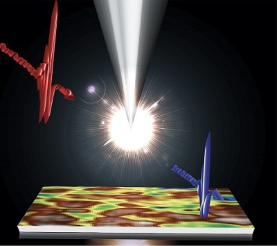 Visualization of the microscope tip exposing material to terahertz light. The colors on the material represent the light-scattering data, and the red and blue lines represent the terahertz waves. Source: U.S. Ames National Laboratory
The microscopy method was applied to the analysis of methylammonium lead iodide (MAPbI3) perovskite, a material that could potentially replace silicon in solar cells This material degrades easily when exposed to heat and moisture, and the researchers predicted MAPbl3 to function as an insulator when they exposed to terahertz light. Instead of the expected consistent low-level of light-scatter throughout the material, large variations in light scattering along the boundary between the grains was observed. The data were indicative to the material’s propensity to degrade under certain conditions.
The data collected document grain boundary and material degradation processes through changes in the levels of light scatterings. The research published in ACS Photonics should prove of value in improving MAPb13 and other materials for photovoltaic applications.