Methods to reduce DC-DC converter output ripple
January 24, 2022From military electronic equipment in weapons systems, unmanned aerial vehicles and radar to aerospace and industrial-grade communications systems, DC-DC converters often require tightly regulated outputs to the load with minimal ripple. The power rails for many modern electronics applications such as networking equipment, high-speed digital communications and industrial Ethernet-connected sensors involving supply voltages that grow smaller (1.2 V, 3.3 V, 5 V) while maintaining the current. This tightens the power requirements of the system where noise-sensitive devices such as high-resolution analog-to-digital converters (ADCs) may require a low output ripple on the order of a few millivolts peak-to-peak (mVp-p) or less. This principle holds true for systems that employ DC-DC converters with higher rated powers and voltages. Any sensitive load device – low noise amplifiers (LNAs), voltage-controlled oscillators (VCOs) and field-programmable gate arrays (FPGAs) – will suffer adverse effects from having high output voltage ripple on the output of a connected DC-DC converter.
VPT, Inc. has specialized in the design and development of DC-DC converters and custom power electronics design services for over 20 years, allowing the customer to leverage their expertise to design robust power systems for an end application. Their products include a wide range of high- reliability DC-DC converters, EMI filters, accessory power products, and custom engineering services for the rapid development of critical power systems, which are designed and engineered to the highest industry standards. This article dives into the various methods to reduce DC-DC converter output ripple, their effectiveness and the considerations that come with these techniques. Several testing approaches are discussed to ascertain both the output ripple at the switching frequency, as well as the level of attenuation seen in its output harmonics.
What is output ripple?
In any DC-DC converter topology, a voltage ripple will occur at the output capacitor. In a forward topology, the current in the inductor is sawtooth and flows through the capacitor to create a voltage ripple. A flyback topology generates a pulsating current that also flows through the output capacitor to create a ripple (Figure 1). The output ripple of the DC-DC converter can include both differential mode currents and common mode currents from parasitic capacitances. Generally, the fundamental switching frequency ripple at the output of the DC-DC converter primarily consists of differential mode noise while the higher frequency spikes are common mode.
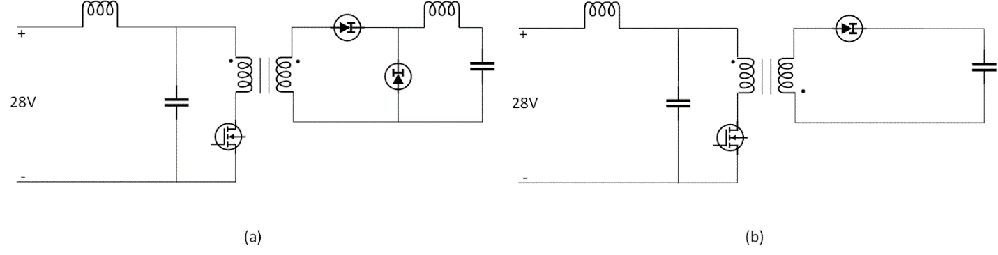 Figure 1: Forward topology (a) and flyback topology (b). Source: VPT, Inc.
The signal appears with both a sinusoidal component generated from the current flowing through the output capacitor as well as higher frequency harmonics due to the power stage switching. These high and low frequency components cause engineers to test voltage ripple across the full bandwidth of the oscilloscope (500 MHz and beyond) in order to observe the high frequency voltage spikes across the output capacitor. Using the oscilloscope’s fast Fourier transform (FFT) function can also be a useful tool for spectral analysis of the output ripple.
Methods for reducing output ripple
Regardless of the topology, a standalone DC-DC converter will carry with it an output ripple that can stand around several hundred millivolts peak-to-peak. However, in many cases this is inadequate to allow the connected circuitry to function properly. In these cases, a second stage must be designed in with either:
- A capacitor-only filter
- An LC filter
- Common-mode choke and capacitor in a Pi-filter configuration
Capacitor-only filter
The addition of a shunt capacitor is the simplest and often most effective form of minimizing the output ripple of the DC-DC converter (Figure 2). The technique of placing a shunt capacitor at the output of the DC-DC converter is practical for filtering out differential-mode current. Each additional component will yield only marginal improvements in the voltage ripple.
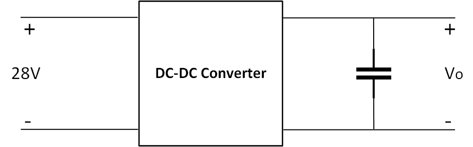 Figure 2: DC-DC converter with a second stage filter consisting of a capacitor with a low ESR. Source: VPT, Inc.
To best optimize the effects of a capacitor-only filter, engineers should employ ceramic capacitors with a good frequency response. Ceramic capacitors with a higher resonant point will reduce the higher frequency ripple much better than tantalum or electrolytic capacitors. Leveraging a simple 1 µF capacitor is often sufficient for suppressing output voltage ripple, however, a designer can go as high as the maximum capacitance listed in the datasheet. Class 1 capacitors such as the C0G or NP0 have the best capacitance stability over temperature, applied voltage and aging but come with the trade-off of a larger size than Class 2 capacitors. Class 2 capacitors leverage more temperature sensitive ceramic materials but can be chosen for more optimal temperature characteristics. The X7 Class 2 capacitors, for instance, operate at over the widest temperature range from -55° C to 125° C while the Y5V operates from -30° C to 85° C. The X7R capacitors offer the broadest range of operating temperatures with the least maximum capacitance change over temperature (+/-15%) — this strikes a balance in size and capacitance stability over temperature. In some cases, the X7S and X7T Class 2 capacitors are also acceptable. Capacitors should be sized to shunt the most troublesome spurious frequency content.
Often, the capacitor’s equivalent series resistance (ESR) is the more important parameter than the actual value of the capacitor for minimizing ripple current. Capacitors must also be placed close to the DC-DC converter output and ensure the return path is a low impedance path. Another major consideration when placing output capacitors is the potential to destabilize the internal control loop of the DC-DC converter.
Engineers must not exceed the total allowable output capacitance specified in the product specification as it can interact with the feedback control loop of the converter.
Capacitor and LC filter
Another option for minimizing the output ripple of the converter is by employing an additional LC filter at the output (Figure 3). This acts as a second-order low pass filter that is more effective at attenuating the output ripple. However, the corner frequency of this LC filter is a serious consideration to avoid failures from destabilizing the internal control loop. It is critical to ensure that the corner frequency is not too low. A general rule of thumb is to make sure the corner frequency is greater than 10kHz to not ensure interaction with the control loop. The inductor should also be rated to handle the load current and its DC resistance (DCR) must be low enough so that the load current does not generate a significant voltage across it.
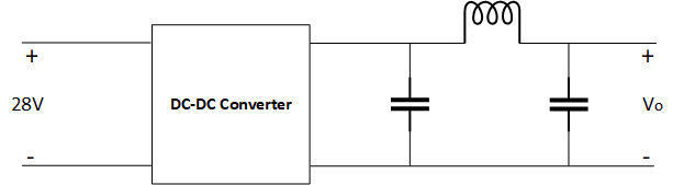 Figure 3: Adding an LC filter onto the output of the DC-DC converter can further suppress both low frequency and high frequency output ripple. Source: VPT, Inc.
Common mode choke and capacitor in Pi-filter configuration
For the best ripple attention, a common mode choke and two capacitors in a Pi-filter configuration is the most ideal option (Figure 4). Common mode chokes are constructed of two independent coils of the same size and number of turns, commonly wound around a toroidal core. This allows the differential signal to pass but reduces common-mode noise. The leakage inductance of the common mode choke and capacitors will create a differential mode filter. To ensure the filter does not interact with the control loop this corner frequency should be greater than 10kHz.
As with any secondary stage filtering in a converter, the amount of noise reduction depends upon the load the DC-DC converter is driving. Both LC and common-mode filtering are less effective at suppressing high frequency components as the load impedance rises. This is a serious consideration for systems with a varying load impedance and will dictate the component values a particular application requires.
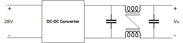 Figure 4: DC-DC converter with a common-mode choke and two capacitors (Pi-Filter) connected at the output. Source: VPT, Inc.
Testing for output ripple
The following tests were output ripple were performed on VPT’s 15W and 30W VXR lineup of high reliability (hi-rel) commercial off-the-shelf (COTS) DC-DC converters. The measured filter performance results will vary depending upon the component layout, temperature, inductors/capacitors used, high frequency characteristics and load impedance. The VXR series of DC-DC converters feature an ultra-wide input voltage range, a high efficiency, and an epoxy-encapsulated packaging that is resistant to chemicals, solvents and salt environments. These DC-DC converters provide a good output voltage ripple performance, however, the addition of the capacitor and common-mode choke with capacitors in a pi-configuration drop output voltage ripple significantly. This allows these components to be used in virtually any high-reliability application with tight tolerances of output ripple.
Method 1: Using a high impedance probe
Testing for the output ripple of the DC-DC converter can be accomplished using either the high impedance probe or the low impedance probe technique. Incorrect probing can easily result in inaccurate ripple results so there are some key considerations when utilizing either one of these methods. The measured filter performance results will vary depending upon component layout, ambient temperature, inductor and capacitor high frequency characteristics as well as the load impedance.
The high impedance probe technique leverages the 10 MΩ oscilloscope probe at the output of the converter (Figure 5). Engineers may be tempted to use the probe’s clip-on ground lead; however, a short ground lead is essential for accurate ripple measurements. The long ground connection of the probe creates a loop that couples in noise to the ripple measurements. The very same reasoning can be applied to the probe’s cabling where the cord should be routed away from the converter and any other source of EMI to mitigate the risk of introducing noise into the test results.
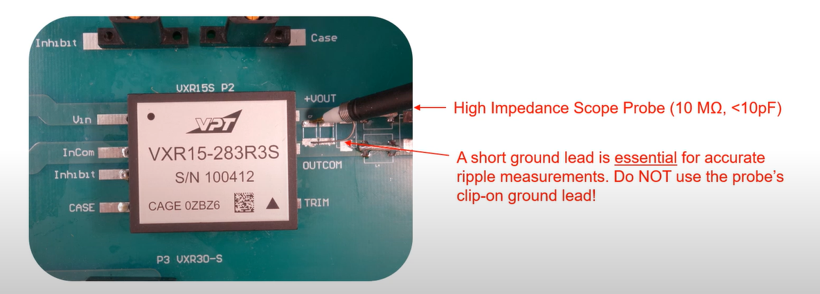 Figure 5: High impedance probe technique using the oscilloscope’s 10:1 probe to measure the output ripple. The use of a short ground lead is essential for producing accurate measurement results. Source: VPT, Inc.
Method 2: Using a low impedance probe
In the low impedance probing technique, the oscilloscope is set to 50 Ω and connects to the output of the converter via a DC blocking capacitor, 50 Ω coaxial cable and a 50 Ω resistor (Figure 6). Using this method, the results must be multiplied by two to compensate for the 2:1 voltage division. It is paramount that the oscilloscope termination be set to 50 Ω. Many engineers often make the error of forgetting this step and are left confused by the characteristic ringing of the waveform at full load. This is due to the creation of a λ/4 resonator where the 50 Ω coax is being terminated into a high impedance load, introducing high-order resonant modes (λ/4, 3λ/4, 5λ/4) into the measurements.
It is important to ensure that all the capacitors have the required voltage rating to ensure that the oscilloscope will be suitably buffered from DC signals.
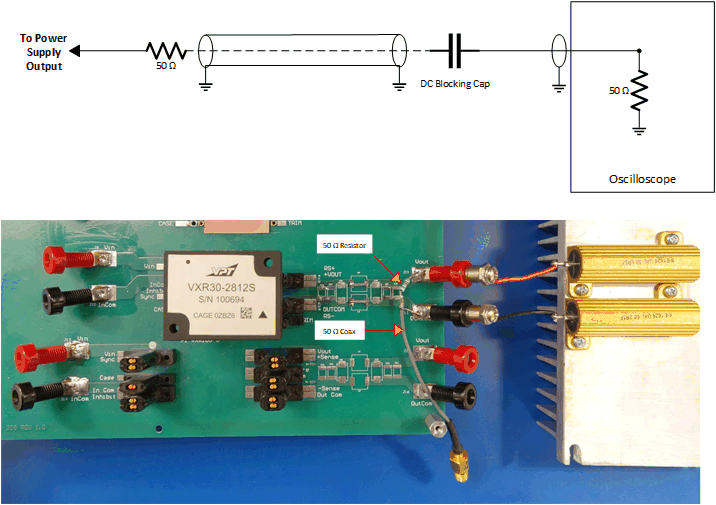 Figure 6: Low impedance probe technique with coaxial cable terminated to the 50 ohm oscilloscope. When done properly, this method is less susceptible to radiated EMI. Source: VPT, Inc.
Using frequency domain plot
In cases where the high-frequency content is vitally important to gauge, a frequency domain plot can be a useful tool. Using the oscilloscope’s FFT function can help an engineer identify output frequencies and power levels that require filters. It is important to fill the oscilloscope’s time record with at least 50 on/off switch transitions for a sufficient resolution. For example, a 500 kHz switching speed would require a 100 µs of time record. The sample rate should also be high enough to prevent aliasing at the high end of the spectrum.
Figure 7 shows the frequency domain plots for the VRX15 DC-DC converter with a 1 µF shunt capacitor as well as a common mode choke and 1 µF capacitor in Pi-filter configuration. It is readily apparent that the harmonics of the switching frequency have all been drastically reduced in the latter configuration. However, the spurs are attenuated by around 15 to 20 dB with the shunt capacitor configuration.
 Figure 7: Frequency domain plot of the VXR15 for both the shunt capacitor and common mode choke configurations. Source: VPT, Inc.
Conclusion ― Comparing the efficacy of these three voltage ripple suppression methods
Depending upon the requirements of the application, various methods can be employed to minimize the output ripple of a DC-DC converter. Capacitor-only filters offer the simplest solution and can cut the voltage ripple almost by a factor of 10. However, these filters are the least successful at suppressing the harmonics of the voltage ripple. To better attenuate the high frequency content of the voltage ripple, the capacitor with the LC filter or the common mode choke and capacitor in Pi-filter topologies are more effective. The common mode choke configuration offers the best high frequency attenuation while also massively reducing the sinusoidal component of the voltage ripple down to a few millivolts peak-to-peak. The type of solution a design engineer employs depends heavily on the available board real estate, cost, time-to-market, and ultimately the noise and sensitivity requirements of the connected electronic components.
With space qualified, mil-spec, high reliability (hi-rel), and high temperature DC-DC converters, VPT, Inc. devices have amassed proven field hours of operation with the majority of the world’s airlines, defense, space contractors and military agencies as well as medical, telecom and electronic equipment manufacturers. For more information about VPT and its products, visit VPT’s website today.
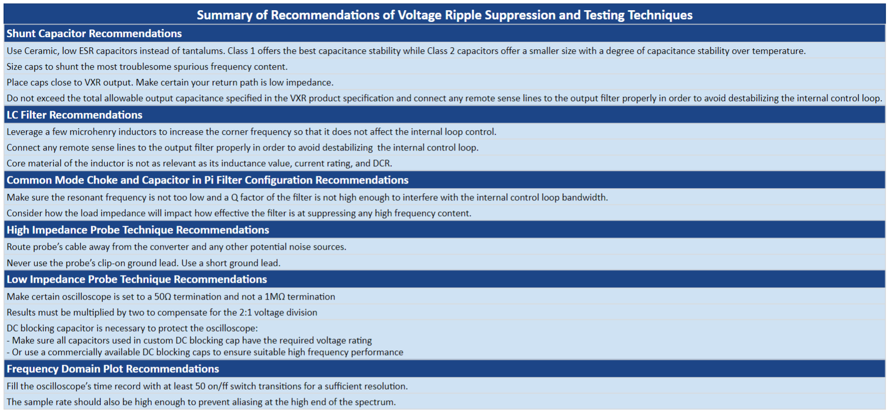 Figure 8: Summary of recommendations of voltage ripple suppression and testing techniques. Source: VPT, Inc.


