Low-cost Method Textures Multicrystalline Silicon Wafers
S. Himmelstein | March 24, 2018An effective method for texturing diamond-wire sawn (DWS) multicrystalline silicon wafers at low cost has been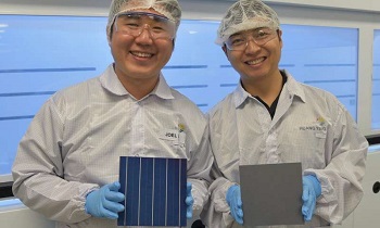 SERIS inventors holding textured DWS multicrystalline silicon solar cell and wafer. Source: NUS demonstrated by researchers from the Solar Energy Research Institute of Singapore (SERIS) at the National University of Singapore (NUS). Texturing roughens the silicon wafer surface to minimize front surface reflection, enhance light trapping and boost solar cell efficiency.
The new wet-chemical technique can supplant available texturing methods which are expensive or result in lower cell efficiencies. The wafer surface is etched with proprietary chemicals to form nanoscale features with dimensions smaller than the incident light wavelength. These structures increase the potential of light having multiple bounces off the surface. The researchers applied the technique to realize solar cells with efficiencies of 20 percent, which is about 0.5 percent higher than those currently mass produced in the factories of tier-1 cell manufacturers.
Manufacturers can leverage this technology to switch from slurry-cut to cheaper DWS multicrystalline silicon wafers, which are 5-15 percent cheaper. For a gigawatt factory, this translates to cost savings on the order of $10 million per year for a gigawatt-scale factory.


