Roughing Up Silicon Solar Cells
S. Himmelstein | July 30, 2017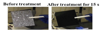 Fabrication of ultralow reflectance polycrystalline silicon wafers. Image credit: Osaka UniversityThe twin goals of containing solar cell costs while maximizing efficiency may be more attainable with silicon technology advanced by researchers from Osaka University, Japan. A 19.8 percent conversion efficiency has been achieved by formation of a nanocrystalline silicon layer on the front surface and a submicron-textured reflector on the rear surface of monocrystalline silicon solar cells.
Instead of using expensive antireflective coatings to boost efficiency, the team chemically treated the front side of silicon cells to produce tiny submicron silicon structures. Application of this surface structure chemical transfer method prevents light reflection and gives the silicon a black appearance.
A method to passivate the submicron silicon structures with huge surface areas was also developed to prevent recombination loss by deposition of phosphosilicate glass followed by heat treatment. The technique simultaneously forms pn-junctions to separate photo-generated electrons and holes.
Rougher light-trapping microstructures formed on the back side of silicon cells increase the capture of infrared light. Due to this light trapping effect, the short-circuit photocurrent density of the nanocrystalline silicon solar cells has been improved to 41.6 mA cm−2.


