Researchers Create Artificial Materials, Atom-by-Atom
Engineering360 News Desk | March 28, 2017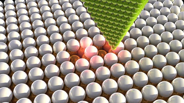 The tip of a scanning tunneling microscope (STM) above chlorine atoms that have been deliberately moved. By moving individual atoms under their microscope, scientists were able to arrange vacancies in a single layer of chlorine atoms and create atomic lattices with a predetermined electrical response. Image credit: Ella Maru Studio and Aalto UniversityResearchers at Aalto University have manufactured artificial materials with engineered electronic properties. By moving individual atoms under their microscope, the scientists were able to create atomic lattices with a predetermined electrical response. The possibility to precisely arrange the atoms on a sample bring “designer quantum materials” one step closer to reality. By arranging atoms in a lattice, it becomes possible to engineer the electronic properties of the material through the atomic structure.
Working at a temperature of four degrees Kelvin, the researchers used a scanning tunneling microscope (STM) to arrange vacancies in a single layer of chlorine atoms supported on a copper crystal.
According to researchers, the correspondence between atomic structure and electronic properties is what happens in real materials as well, but here there is complete control over the structure. In principle, researchers could target any electronic property and implement it experimentally.
Using their atomic assembly method, the research team demonstrated complete control by creating two real-life structures inspired by fundamental model systems with exotic electronic properties.
The approach is not limited to the chlorine system chosen by the research team either. The same method can be applied in many well-understood systems in surface and nanoscience and could even be adapted to mesoscopic systems, such as quantum dots, which are controlled through lithographic processes.