Method to Dissipate Heat in Electronic Devices
John Simpson | November 21, 2016Controlling the flow of heat through semiconductor materials is a challenge in developing smaller and faster computer chips, high-performance solar panels and better lasers, and biomedical devices.
An international team of scientists has modified the energy spectrum of acoustic phonons—elemental excitations, also referred to as quasi-particles, that spread heat through crystalline materials like a wave—by confining them to nanometer-scale semiconductor structures. The results have implications in the thermal management of electronic devices.
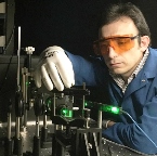 Fariborz Kargar, a graduate student researcher at UCR, measures the acoustic phonon dispersion in the semiconductor nanowires. Image credit: UCRLed by Alexander Balandin, professor of electrical and computing engineering at the University of California, Riverside, the researchers used semiconductor nanowires from gallium arsenide (GaAs), synthesized by researchers in Finland, and an imaging technique called Brillouin-Mandelstam light-scattering spectroscopy to study the movement of phonons through the crystalline nanostructures. By changing the size and the shape of the GaAs nanostructures, they were able to alter the energy spectrum, or dispersion, of acoustic phonons.
Controlling phonon dispersion is crucial for improving heat removal from nanoscale electronic devices, which has become the major roadblock in allowing engineers to continue to reduce their size. It can also be used to improve the efficiency of thermoelectric energy generation, Balandin says. In that case, decreasing thermal conductivity by phonons is beneficial for thermoelectric devices that generate energy by applying a temperature gradient to semiconductors.
“For years, the only envisioned method of changing the thermal conductivity of nanostructures was via acoustic phonon scattering with nanostructure boundaries and interfaces," Balandin csays. "We demonstrated experimentally that by spatially confining acoustic phonons in nanowires, one can change their velocity, the way they interact with electrons and magnons and how they carry heat. Our work creates new opportunities for tuning thermal and electronic properties of semiconductor materials."


Back in my short flirtation with EE, in EE 101 lab, we did our first breadboard, consisting of about 15 components. What a sloppy mess. It looked so neat and clean on paper. Instead of going on to the next circuit, the prof said. ''OK, clean it up and do it again, making your second try more conspicuously efficient.''
Having zero social life that year, I sweated it over a weekend to redo the circuit in a very tedious and painful cut and paste of breadboard pieces to make the circuit in three vertical breadboard tiers. By appearance (e. g., the planes of the three levels were significantly tilted compared to each other and horizontal), it was uglier than my first single plane breadboard.
But it got the prof's attention...and a lot of laughs at my expense. I was commended for an effort that had no relevance to the real world of (electronic) circuits: The bottom line was, if for no other reason, such 3D circuits were ultimately constrained by heating.
Decades later, it seems we are still up against the heat issue for 3D, even if additive manufacturing may be able to build compact fully integrated 3D electrical/electroni