Reliability in electronics through informed material choices
July 10, 2025Product security and reliability are major concerns in the semiconductor and PCB fabrication industries. Because of this, electrical or wafer-level testing and material traceability are key areas of focus. Material selection is often overlooked, though, despite being a critical step in the process. Suppliers frequently source materials without considering how they might interact, which inevitably leads to compatibility issues.
Material compatibility issues can cause short-term failures or a reduced operational lifetime for the device, whether at the wafer-level processing stage or during circuit board manufacturing. There are methods to easily incorporate synergistic materials that prevent these compatibility-related failures in both semiconductor and PCB fabrication and assembly. These strategies allow manufacturers to avoid stringent materials selection and testing processes.
Defining reliability in electronics
The endeavor to analyze failures from the wafer-level circuit and layout design, fabrication, packaging and test; all the way up to PCB design, circuit and layout design, fabrication and test; is exceedingly intricate. An array of parameters causes these failures. For semiconductors, this depends on choice of substrate, oxide, metallization, bonding and packaging. For PCBs, variabilities in layout topologies, choice of laminate, stackup and via design can introduce avenues for failure. In electronics manufacturing, failures for products that are produced en masse will eventually follow trends that can be modeled statically.
Bathtub curve
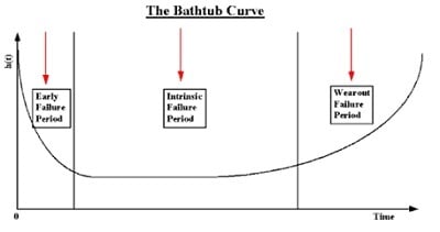 Figure 1. Bathtub representation of electronic component failure rate over time. Source: NIST
In the field of reliability, the bathtub curve is the most famous statistical representation of failures over the lifetime of a population of electronics components (Figure 1). The curve describes a general lifetime pattern with a premature failure rate that decreases with time; a useful life with constant (random) failures; and a longterm wear out with a rapidly increasing failure rate with time. These failures can be broken into two quantifiable categories: intrinsic and extrinsic.
Intrinsic and extrinsic failures
Intrinsic failures are natural macro-defects or device deteriorations that occur in a normal fabrication or assembly process functioning within specification limits. Intrinsic failures are also generally responsible for many of the earliest failures; however, they can also contribute to long-term device wear out. As its name implies, intrinsic failures are uncontrollable while extrinsic failures are within the manufacturer’s control.
Extrinsic failures typically surface during the early failure period of the bathtub curve and are a direct result ofmanufacturing defects or errors introduced during the design, layout, fabrication or assembly stages. These failures often manifest under excessive electrical, thermal, mechanical or radiative stress.
To detect these failure modes early on, manufacturers frequently employ “burn-in” testing before product deployment. These failures present challenges like voids, delamination or die cracking at the die attach interface, and mitigating them requires robust quality control measures. The manufacturer is often responsible for tracking, monitoring and control of both intrinsic and extrinsic failures during the assembly and fabrication process. Quality control strategies to improve yields vary per vendor. For example, many leverage the Lean Six Sigma methodology, define-measure-analyze-improve-control (DMAIC), to assist in improving yields.
Yield improvement in manufacturing and assembly processes often necessitates fine-tuning procedures that are highly specific to those processes. Thoroughly analyzing material choices is essential to optimize the creation of complex products such as smartphones and automotive equipment. This evaluation should begin at the foundational chip production level, through semiconductor packaging, and extend upwards to the PCB fabrication, assembly and packaging stages.
Material compatibility in semiconductor assembly
The major extrinsic failure modes that arise during semiconductor assembly are often related to die attach – or die bonding – technologies. These issues grow in importance at higher power levels where thermal Figure 2. Typical semiconductor assembly with chip, DBC substrate and case. Source: MacDermid Alpha management becomes crucial.
In Figure 2, power devices — such as insulated gate bipolar transistors (IGBTs), super junction metal-oxide-semiconductor field-effect transistors (SJ MOSFETs), silicon carbide field-effect transistors (SiC FETs) and gallium nitride high-electron-mobility transistors (GaN HEMTs) — should pass the initial round of checks to be considered “good die.” They are attached to a direct bond copper (DBC) substrate often composed of a ceramic material such as alumina and aluminum nitride, or a copper leadframe. The chip and DBC are then attached to the case or baseplate which is typically metal or a composite material. At this point, it is possible to bond this entire assembly to a heatsink to effectively increase the surface area and radiate excess heat.
Maximizing heat transfer
It is critical to optimize thermal resistance at the various material interfaces and closely match the coefficient of thermal expansion (CTE) between materials. This maximizes heat dissipation from the power device all the way down to the heat sink. A significant CTE mismatch between the die and the substrate leads to mechanical stress, potentially causing delamination or cracking since dissimilar materials expand and contract at different rates when exposed to temperature changes.
Chip interface considerations
There are significant mechanical constraints at the interface between the chip and DBC. The materials employed for die attach must prevent weak bonds that fail under thermal cycling or mechanical stress. Voids within the die attach layer can also function as thermal and electrical insulators, reducing the overall performance of the device.
Wide bandgap (WBG) materials such as SiC have exacerbated the number of potential mechanical failures that occur during thermal cycling. During power cycling, conventional silicon dies exhibit flexure, resulting in less strain on the connected die attach material. However, SiC is three times stiffer and thus a more brittle material, causing most of the strain from power cycling to be placed on the die attach layer.
Die attach technologies can vary between soldering and sintering. The sintering process typically involves the use of silver-based pastes that, when heated and under pressure, form a high-thermally conductive bond. However, hybrid silver sintering technology (HSST) has emerged as a strong option for WBG die attach due to its excellent power cycling endurance.
HSST uses micron-sized silver powder and an organic material. The unique design of the polymer composition facilitates silver sintering at low temperatures without pressure during the curing process. This achieves high thermal conductivity and overcomes the limitations of conventional silver sintering products.
However, these materials need to be carefully formulated to minimize voiding. Ideally, die attach processes must be compatible with existing manufacturing processes. This includes considerations for curing temperatures, pressure requirements and the ability to manage different die sizes and thicknesses.
Semiconductor fabrication and packaging are filled with use cases where material compatibility can be better assessed to yield a more robust end product. This concept of careful materials selection extends out to PCB fabrication.
Material compatibility in PCB fabrication
 Figure 3. Basic PCB fabrication process. Source: MacDermid Alpha
Board design, layer count and laminate material choices influence the complexity of PCB fabrication. These factors are important considerations when manufacturing standard multilayer rigid PCBs, high density interconnect (HDI) PCBs or high-frequency application circuit boards. The fabrication process for standard PCBs is shown in Figure 3.
Inner layer processing
Inner layer processing consists of a develop, etch and strip (DES) process. The core material – typically a laminate with copper on either side – is cleaned in an acid dip and coated in photoresist for the development of a layer-specific circuit pattern. The exposed circuit pattern is maintained while the rest is etched away. After all the inner layers are complete, they are laminated and “pressed” together to form a multilayer PCB.
Drilling
After the DES process, drilling begins. Mechanical or laser drills can be used depending on the aspect ratio (a measure of the ratio of via depth to via diameter) of the via. For instance, microvias are laser-drilled structures often found in HDI PCBs with a tightly controlled width and limited depth. After the holes are drilled and cleaned, the board moves to the primary metallization process.
Primary metallization
Primary metallization typically uses either electroless copper plating or direct metallization (DM) to deposit a thin conductive layer that is built up with copper to a specific thickness with electrolytic copper plating. Electroless copper deposits a copper coating from the solution through chemical reduction, while DM deposits a carbon- or graphite-based conductive coating through absorption onto the surface. Electroless copper processes consume more water, energy, and chemicals while utilizing a larger floor space and therefore have a larger carbon footprint than DM. Today, many PCB manufacturing facilities are replacing  Figure 4. Manufacturing processes must deposit the seed layer on difficult-to-plate substrates while also minimizing CTE mismatches and providing a stable base for more metallization. Source: MacDermid Alpha electroless copper processes with DM, due to its reliability and clear environmental and cost benefits.
This seed layer is critical to ensure good adhesion to the exposed inert via surfaces (and other structural designs) and uniformity for subsequent plating. Core materials may vary, often causing manufacturers to fall out of spec with difficult-to-plate substrates (Figure 4). Properly controlled primary metallization processes can minimize CTE mismatches, providing a stable base for further metallization.
Electroplating
At this stage, the outer layer image is transferred to the outer panel, revealing a copper pattern plated with electrolytic copper. This process develops the conductive layers on the seed layer, ensuring robust electrical pathways. The formulation of this material is crucial, as it must fill vias while plating fine lines, pads and other surface features with high coplanarity and low trace profiles. Additionally, the electrolytic copper layer adds mechanical strength to the substrate, enabling it to endure stresses from larger die sizes and high aspect ratio through holes. The outer layer is stripped and etched in preparation for the final finishes.
Finishes
To ensure reliable electrical connections, final finishes like Electroless Nickel-Immersion Gold (ENIG), Immersion Tin (ImSn), Immersion Silver (ImAg), or Organic Solderability Preservative (OSP) are essential. These finishes protect the copper layers from oxidation and corrosion while ensuring good solderability. High-quality finishes also maintain signal integrity by providing smooth, uniform surfaces for high-frequency signal transmission. Manufacturers can ensure reliable and high-performance IC substrates by carefully selecting and controlling these processes to address the challenges associated with larger die sizes, increased I/O counts, thicker boards and high aspect ratio holes.
Materials compatibility in PCB assembly
The PCB assembly process is also filled with opportunities to optimize material interfacing to improve product reliability.
BGA assembly for board-level reliability
Achieving board-level reliability requires a holistic evaluation of the entire assembly design rather than relying solely on pass/fail electrical tests or visual inspections. By examining the full system, engineers can identify stress accelerators — such as thermal mismatches, mechanical strain, and material incompatibilities — that compromise long-term performance. This approach is especially critical when integrating fine-pitched components like ball grid arrays (BGAs) or chip scale packages (CSPs), which are more susceptible to failure under thermal and mechanical stress. Through strategic selection of high-reliability solder pastes with the Innolot® Alloy and reinforcement polymers—such as underfills and edgebonds — manufacturers can mitigate these stressors, enhance thermal fatigue resistance, and ensure the component remains securely attached. This integrated materials-driven strategy enables targeted reliability improvements tailored to the demands of the end application.
BGA failures
Fine-pitch integrated circuits (ICs) such as ball grid arrays (BGAs) demand greater design consideration than standard surface mount devices due to their heightened sensitivity to both mechanical and thermal stresses. BGAs are particularly vulnerable to mechanical failures caused by high-stress events like drop shock and impact bending. These sudden forces can induce brittle fractures or ductile tearing in solder joints, especially when the PCB flexes or experiences abrupt deceleration. Factors such as board thickness, component mass, and solder joint geometry significantly influence the likelihood of failure.
Additionally, BGAs are more susceptible to board strain (e.g., curvature or warpage), which can impose further stress on solder joints. To mitigate these risks, reinforcement strategies such as underfills and edgebonds are commonly employed. These polymer materials fill the gaps between the chip and the PCB substrate, and once cured, they help distribute mechanical loads, reduce strain on solder bumps, and protect the component from environmental contaminants. Together, these measures improve the mechanical resilience of BGA assemblies and contribute to overall board-level reliability.
In contrast, thermal cycling introduces a different failure mechanism—creep deformation—driven by repeated expansion and contraction of dissimilar materials. Over time, this leads to fatigue cracking in solder joints, particularly when there is a significant CTE mismatch between the package and the PCB. This failure mode is gradual and accumulative, often manifesting after hundreds or thousands of cycles. To combat this, high-reliability solder alloys, such as Innolot® with enhanced creep performance and reinforcement materials like underfills are employed to absorb thermal stresses and extend the operational life of the assembly.
Reinforcement polymer and solder considerations
The large surface area and number of solder joints in BGAs call for both high-reliability solder pastes and reinforcement polymers to ensure the component remains attached (Figure 5).
Epoxy-based edgebonding materials with high glass transition temperatures (Tg) improve the ability to pass stringent TCTs. A higher Tg would equate to a more stable structure at higher temperatures. When combined with a high-reliability solder paste, the thermal fatigue resistance of the component increases dramatically. As such, well-formulated solder alloys exhibit minimal creep during TCTs, showing high thermomechanical stability and thus high reliability.
Carefully choosing solder pastes and reinforcement polymers for challenging components, such as BGAs, is only one aspect of improving PCB assembly. Optimizing every aspect of PCB assembly materials selection improves the electrical, thermal, mechanical and environmental performance of the board.
A bottom-up approach to materials optimization
 Figure 5. Reinforcement polymers as applied and with the BGA attached. Underfills use capillary flow to fill all spaces between the die, substrate and and bumps. Source: MacDermid Alpha
Material incompatibilities are often the source of intrinsic and extrinsic electronics failures, both at the chip and board levels. At each step within the fabrication, assembly and packaging
process, thoughtfully chosen specific materials not only mitigate the costly impacts of early failures but also maximize the field life of an electronic system.
It is best to take a bottom-up approach to materials, flexibly selecting and deploying the most ideal materials based on the requirement of the end application. This allows the manufacturer to preemptively consider how the space, cost constraints, environmental stressors and electrical performance can all be improved. Given the fast pace of electronic advancements, it is important to rapidly shift from design concept to working prototype to a finalized product without compromising reliability.
MacDermid Alpha Electronics Solutions (MAES), a global leader in fully integrated materials, empowers electronics assemblers, PCB fabricators and in-mold electronics manufacturers to improve product performance, reliability and sustainability.
Trusted by manufacturers in over 50 countries and backed by a century of innovation, MAES is uniquely positioned to deliver high-quality materials solutions from die fabrication all the way up to PCB assembly. MAES’s legacy and expertise have actively shaped many modern technology segments, including automotive, consumer electronics, mobile devices, telecom, data storage, and infrastructure. Contact MAES today to learn how they can optimize the entire supply chain.