New Transistor Could Open Door to Flexible Electronics
By Engineering360 News Desk | March 14, 2016A team of research engineers from the University of Alberta (UA) has invented a new transistor that could open the door to the development of flexible electronic devices in applications as wide-ranging as display technology, medical imaging and renewable energy production.
Efforts by researchers to improve the performance of thin-film transistors (TFTs), of the sort commonly found in low-power, low-frequency devices like display screens, to date have been slowed by the challenges of developing new materials for use in these applications.
Rather than develop new materials, a UA electrical engineering team led by PhD student Gem Shoute improved their performance by designing a new transistor architecture that takes advantage of bipolar action. Instead of using one type of charge carrier, as most TFTs do, it uses electrons and the absence of electrons (referred to as “holes”) to contribute to electrical output.
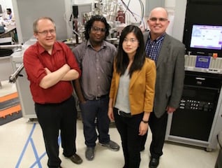 UA researchers (l-r): Doug Barlage, Triranta Muneshwar, Gem Shoute and Ken Cadien. Image credit: University of Alberta.Their first breakthrough was forming an "inversion" hole layer in a wide-bandgap semiconductor, which has been a great challenge in the solid-state electronics field. Once this was achieved, “we were able to construct a unique combination of semiconductor and insulating layers that allowed us to inject 'holes' at the [metal oxide semiconductor] interface,” says Shoute.
Adding holes at the interface increased the chances of an electron “tunneling” across a dielectric barrier. Through this phenomenon, a type of quantum tunneling, the group was able to achieve a transistor that behaves like a bipolar transistor.
“It’s actually the best-performing [TFT] device of its kind,” says fellow researcher and materials engineering professor Ken Cadien. “This kind of device is normally limited by the non-crystalline nature of the material that they are made of.”
The transistor has power-handling capabilities at least 10 times greater than commercially produced TFTs. Moreover, the dimensions of the device itself can be scaled with ease in order to improve performance and keep up with the need for miniaturization, an advantage that modern TFTs lack.
UA electrical engineering professor Doug Barlage says the group's goal was to make a TFT with the highest power handling and switching speed possible. "Not many people want to look into that, but the raw properties of the film indicated dramatic performance increase was within reach,” he says.
In the end, the team took advantage of the very phenomenon that other researchers considered roadblocks.
“Usually tunneling current is considered a bad thing in [metal oxide semiconductor field effect transistors] and it contributes to unnecessary loss of power, which manifests as heat,” explains Shoute. “What we’ve done is build a transistor that considers tunneling current a benefit.”
The team has filed a provisional patent on the transistor. Shoute says the next step is to put the transistor to work in a fully flexible medium and apply such a device to biomedical imaging or renewable energy applications.


