Kinwong’s PCB development trends and solutions
January 26, 2021With the rapid development of electronic technology in recent years, printed circuit board (PCB) products are pursuing higher heat dissipation capabilities, with high voltage and high current characteristics, and are developing high-density interconnection (HDI) technology.
Kinwong is a PCB manufacturer headquartered in Shenzhen, China, with 28 years of manufacturing experience, and ranks 20th in the PCB industry globally. Kinwong has multiple technology manufacturing capabilities, such as PCB, flexible PCB, metal base PCB, substrate-like PCB and high layer count PCB.
When faced with COVID-19, Kinwong’s quick adaptations achieved revenue of more than $1 billion in 2020. Kinwong has nine factories in the four major production bases in China, employs 12,500 people worldwide and provides global, localized business development and FAE support. Kinwong partners with numerous top global brands and has earned an excellent reputation.
In the field of automotive circuit boards, Kinwong is the number one PCB manufacturer in China in terms of revenue, and internationally Kinwong ranks tenth.
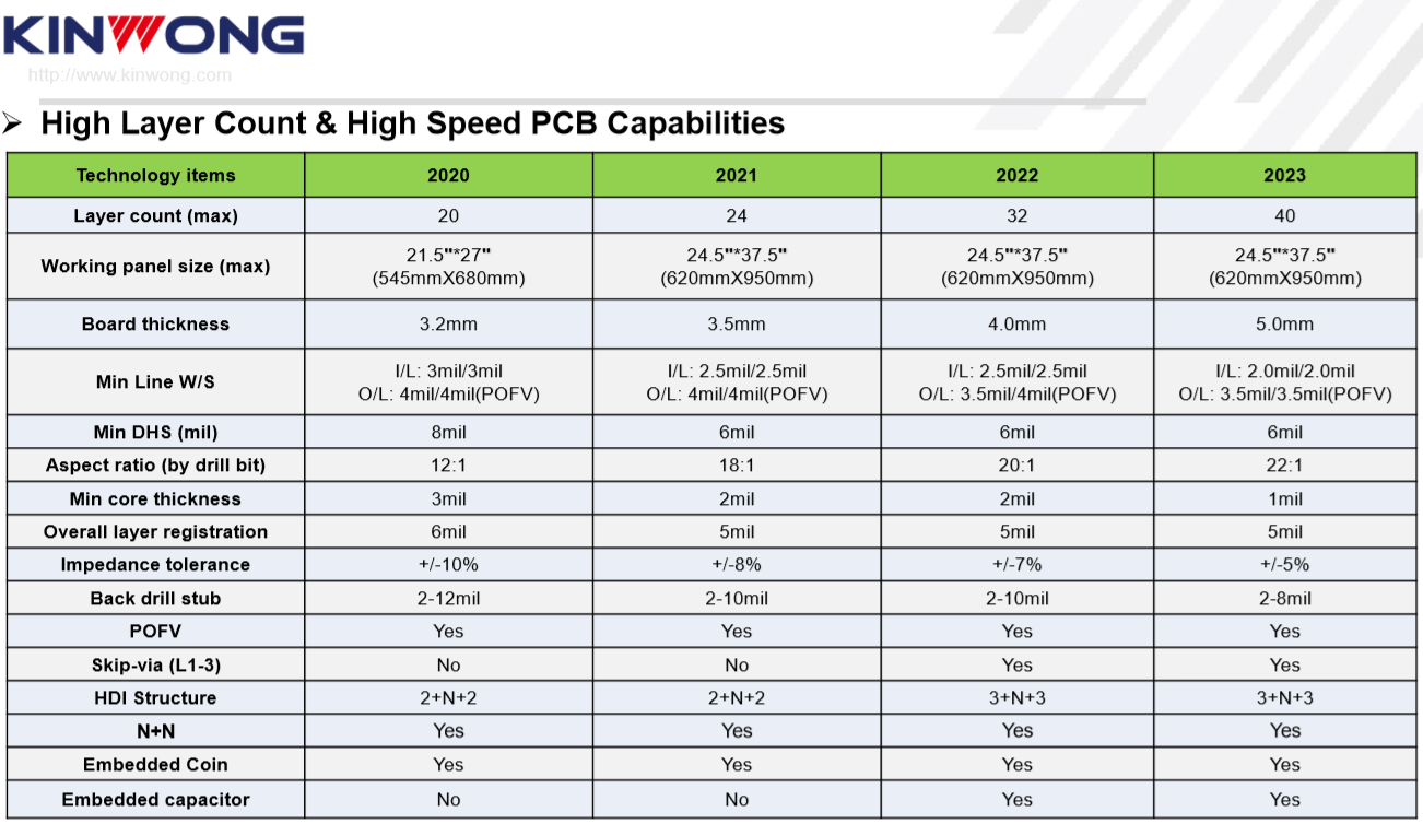 Figure 1. Kinwong’s current and planned high layer count and high-speed PCB capabilities. Source: Kinwong
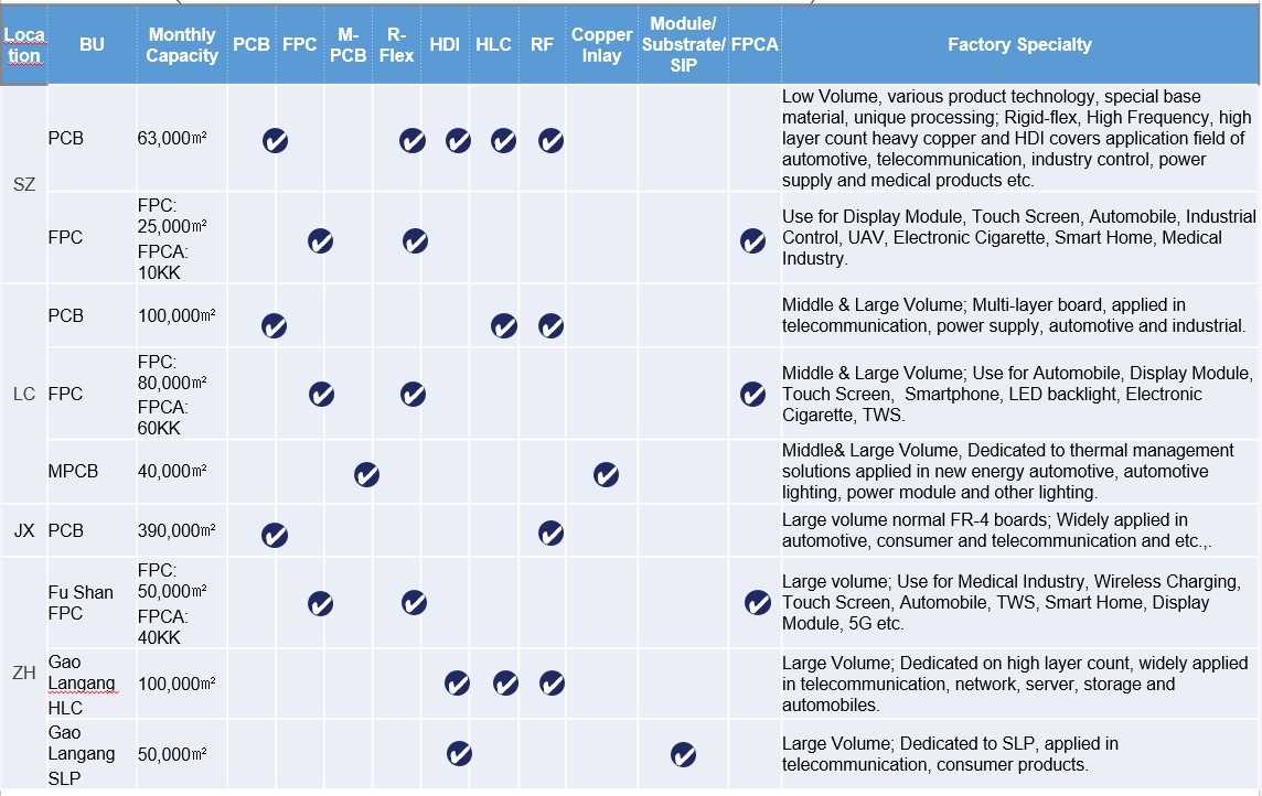 Figure 2. The manufacturing capabilities of Kinwong's nine factories. Source: Kinwong
Automotive Development trend: E-mobility
- High power
- High voltage
- High current
- Thermal management solution
Kinwong’s solutions
- Copper/aluminum-based insulated metal substrate
- Copper pedestal
- High thermal conductivity
- Excellent thermal performance
- Good electrical performance
- Heavy copper
- Less thermal stress
- Maximum 6 oz base
- UL recognized
- Copper/AIN Inlay
- “I,” ”T,” ”U”-shaped Cu coin
- Maximum ±30 µm height performance
Development trend: Advanced driver-assistance systems/autonomous driving
- Higher transmission rate
- Lower loss
Kinwong’s solutions
- High frequency millimeter-wave radar
- HC/PTFE-based raw material
- Hybrid/blind via
- High accuracy copper image pattern(±15um)
- High layer registration (±5mil)
- HDI
- 2+N+2
- 0.65 mm ball grid array pitch (improved in 2021 at Zhuhai factory)
- 60 µm/60 µm trace width/spacing
- Large-size display screen FPC
- More feature-rich
- Last longer
- Longer finger pitch length (greater than 100 mm)
- Surface finish: ENIG
- Drill hole min. 0.1 mm, laser blind via min. 0.05 mm
- Min. trace width/spacing of 45 um/45 um
- Impedance control
- Battery management system FPC
- High heat resistance
- High power
- FPC length is more than 1,000 mm
- Copper thickness greater than 2 oz
- 3D stiffener assembly
- Conformal coating for component
5G
- High speed
- Super transmission rate
- Lower loss
Kinwong’s solutions
- High layer count
- Large panel size
- Small hole backed drilled
- POFV
- Skip via
- Impedance control
- Insertion loss
- Optical module
- ENIG/ENEPIG+G/F
- High speed material
- Hybrid
- HDI | N+N | cavity
- Cu inlay
- Segmented/graded G/F
- Tight size tolerance
- Antenna
- 2L~4L
- High frequency material
- Hybrid
- Cavity
- Strict radio frequency trace tolerance antenna
- TRX/PA/Base band/Backplane
- Large size
- Back drilling
- POFV
- Half-plated hole
- Edge plating
Consumer
- High density
- Small hole size
- High capacity
- Light, thin and small
Kinwong’s solutions
- HDI
- 3+N+3
- Analyzer (Zhuhai 2021)
- SLP (Zhuhai 2021)
- mSAP (Zhuhai 2023)
- amSAP (Zhuhai 2023)
- Min. trace width/spacing of 30 um/30 um
- Stack via/stagger via/step via
- Min. board thickness of 0.2 mm
- 5G phones, antenna FPC and transmission line FPC
- PTFE/LCP/MPI-based material
- 3L~4L
- Laser drilled blind via
- Copper filled via
- Impedance control
- Insertion loss control
- Signal simulation
- 3D SUS stiffener
- Unmanned aerial vehicle/UAVs FPC
- L1~6L
- Drill hole min. 0.1 mm, laser blind via min. 0.05 mm
- Min. trace width/spacing of 45 um/45 um
- Surface finish: ENIG, ENEPIG and OSP
- Impedance control
- 3D SUS stiffener
Industrial and medical device
- Long-term reliability
- High stability
- Portable
- Miniaturized
- Intelligent
Kinwong’s solutions
- Rigid-Flex
- ENIG/LF HASL/OSP
- Max.16 L
- Max. 6 L flexible layer count
- Flexible area with different layer count
- CVL at rigid
- HDI
- Gold finger design
- Dispensing
- ±10% impedance control
- Bendable and 3D assembly for small size
- Middle/high Tg base material
- Soldermask plugging
- Semi-flex
- Max. 2L bendable layer
- Bending area thickness, 0.25 mm ± 0.05 mm
- Bending angle 0~180°
For more information, visit the Kinwong website.


