2D solution for next-generation semiconductors
Amy J. Born | July 15, 2020The need for reliable and stable semiconductor memories is growing along with the distribution and streaming of vast amounts of high-quality content. Researchers from the Pohang University of Science and Technology (POSTECH) have developed a next-generation memory device using a two-dimensional layered-structure material.
 Source: POSTECHThe research team sought to create a memory device that would process information at high speeds, store large amounts of data with non-volatile characteristics (information does not disappear when the power is off) and has low power needs for use in mobile devices.
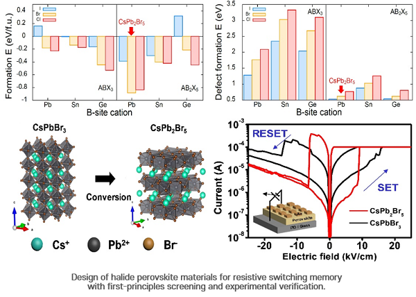
When comparing the relative stability and properties of halide perovskites with other structures, calculations predicted a two-dimensional layered structure may have greater stability than the three-dimensional structure and also have improved performance in memory devices. The results were verified by synthesizing an inorganic perovskite material with a two-dimensional layered structure and applying it to memory devices. The devices with three-dimensional structures lost their memory characteristics when temperatures exceeded 100° C. The devices with a two-dimensional layered structure, however, maintained memory characteristics over 140° C and could operate below 1 V.
"Using this materials-designing technique based on the first-principles screening and experimental verification, the development of memory devices can be accelerated by reducing the time spent on searching for new materials," commented Professor Jang-Sik Lee who led the research. "This is expected to accelerate the commercialization of next-generation data storage devices."
The findings were published in Advanced Science.


