Keys to Choosing Ceramics and Substrates for High-Power Electronics
Engineering360 News Desk | December 10, 2018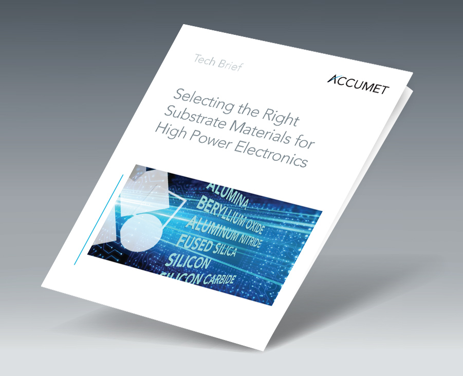 Accumet, an advanced materials processing and assembly partner, has announced the release of their new tech brief, which the company says provides the fundamentals for choosing ceramics and substrates for high-power electronics. Aimed at high power circuit and system designers, the brief details the common ceramic and semiconductor material choices encountered by designers, and offers insight on the advantages, disadvantages and tradeoffs of each so as to allow for informed decision making that leads to ideal performance and yields.
Among the choices for materials utilized in high-power electronics are composite substrates composed of metals and ceramics, as well as insulating semiconductor substrates. The stackup of a high-power device typically includes a ceramic base layer stacked with a semiconductor substrate layer. Thin- and thick-film processes also leverage ceramic materials as a base layer. So the applications and variables are vast, particularly as frequency/power combinations vary from design to design.
Several different ceramic materials, such as alumina (Al2O3), beryllium oxide (BeO), aluminum nitride (AlN), and fused silica are utilized in high power devices as base materials. Semiconductor materials, such as silicon (Si) and silicon carbide (SiC), are semiconductor substrates for high-power gallium nitride (GaN), gallium arsenide (GaAs), Si and SiC power devices.
Each of these materials and substrates has specific characteristics that lend themselves to certain applications, and selecting a ceramic material or substrate is a design decision with substantial ramifications throughout the design/manufacturing/installation process — especially considering that power electronics are often connected and incorporated into complex and expensive systems that depend on long-term reliability and high efficiency. Each material also has its own sourcing and processing requirements, such as possible lapping, polishing or edge grinding requirements for preparation ahead of manufacturing.
The independent and combined attributes of these materials and processes, in consideration of PCB and packaging requirements as well, is where knowledge of material behavior will come in handy.
To download the brief, click here.