New tandem solar cell design reaches 25% efficiency
S. Himmelstein | October 08, 2020Most photovoltaic systems employ silicon solar cells due to their relatively low cost and 20% solar conversion efficiency. Tandem cells have been designed to bolster the efficiency of Si-based devices, which are approaching theoretical efficiency limits. A cost-effective approach to tandem cell fabrication has been demonstrated by researchers from the University of Illinois, Arizona State University and Yale University.
The new method layers the semiconductor material gallium arsenide phosphide onto Si because the two materials complement each other. Both absorb visible light, but gallium arsenide phosphide does so while 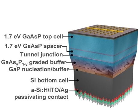 Schematic shows the layered structure of the tandem solar device. Source: Shizhao Fan et algenerating less waste heat.
During fabrication, material defects emerge in the layers, particularly at interfaces between the silicon and gallium arsenide phosphide and can compromise both performance and reliability. This issue was circumvented by replacing the commonly used gallium indium phosphide electron-blocking layer at the back of the cell with a wide-band gap aluminum gallium arsenide phosphide back surface field layer. The inclusion of an additional gallium arsenide phosphide spacer layer ensures more distance between the cell active region and defects in the graded buffer.
The design details published in Cell Reports Physical Sciences resulted in an increase in carrier lifetime and a tandem cell with an efficiency of 25%.