Q&A: A deep dive into pSemi's supercharged portfolio
Emily Councilor | July 07, 2025Over the last decade, pSemi has been transitioning its focus from silicon-on-sapphire (SOS) technology to a silicon-on-insulator (SOI) upgrade, simplifying the power architecture for intricate RF switch technology. Their latest advancement in RF SOI unveils the UltraCMOS+™ semiconductor technology platform, following 16 generations of UltraCMOS development and expanding the usage model while also optimizing performance for targeted RF functions.
 "Launching this next-gen platform to our historical markets will once again change the way our customers design and architect their RF products." Rodd Novak, VP of Sales & Marketing, pSemi
GlobalSpec (GS): What are the biggest differentiators between the previous UltraCMOS generations and the newest UltraCMOS+?
pSemi: UltraCMOS+ represents 16 generations of advancements in RF SOI technology. This includes gate lengths of less than 50 nm — more than 10 times shorter than our first 500 nm UltraCMOS RF switch. Each generation has improved more than one figure of merit and created opportunities to expand our portfolio.
The most significant change is that, while our original approach was to create a single UltraCMOS platform for all products, we now have multiple specialized platforms tailored for different functions, frequencies and power levels. This evolution enables us to mix and match feature sets to create specialty capabilities — possible with UltraCMOS+.
GS: You are a seasoned vet in the RF business. How do you see this further changing the space that pSemi already dominates?
pSemi: UltraCMOS originally targeted monolithic, high-performance RF switch-based products, such as step attenuators, RF switches and switched tuning capacitors. UltraCMOS+ has enabled a portfolio of products that support a full set of integrated RF, analog and digital functions. An example is our latest product for Wi-Fi, Thread and Bluetooth, which combines a high-performance power amplifier, LNA, RF switches, sensors and tuning elements into the industry’s smallest form factor and highest-performance monolithic FEM. Our first products will target the IoT market, which values these differentiating capabilities, but we will be launching additional products prioritized by where UltraCMOS+ can make the biggest impact.
GS: You mentioned at IMS that you’re targeting designers with this new platform. Can you talk more about why it’s important to speak directly to RF designers and engineers?
pSemi: Our solutions are unique and typically enable the designer to change the way they architect their design. As an example, we recently launched a 52 dBm RF switch with nearly 90 dBm IIP3, the PE42448. The linearity of this switch enabled our customer to eliminate a filter and change the system lineup. This is a simple example, but we are now targeting more integrated solutions that can eliminate complexity, size and cost, and improve performance. Keep an eye out for our next announcements.
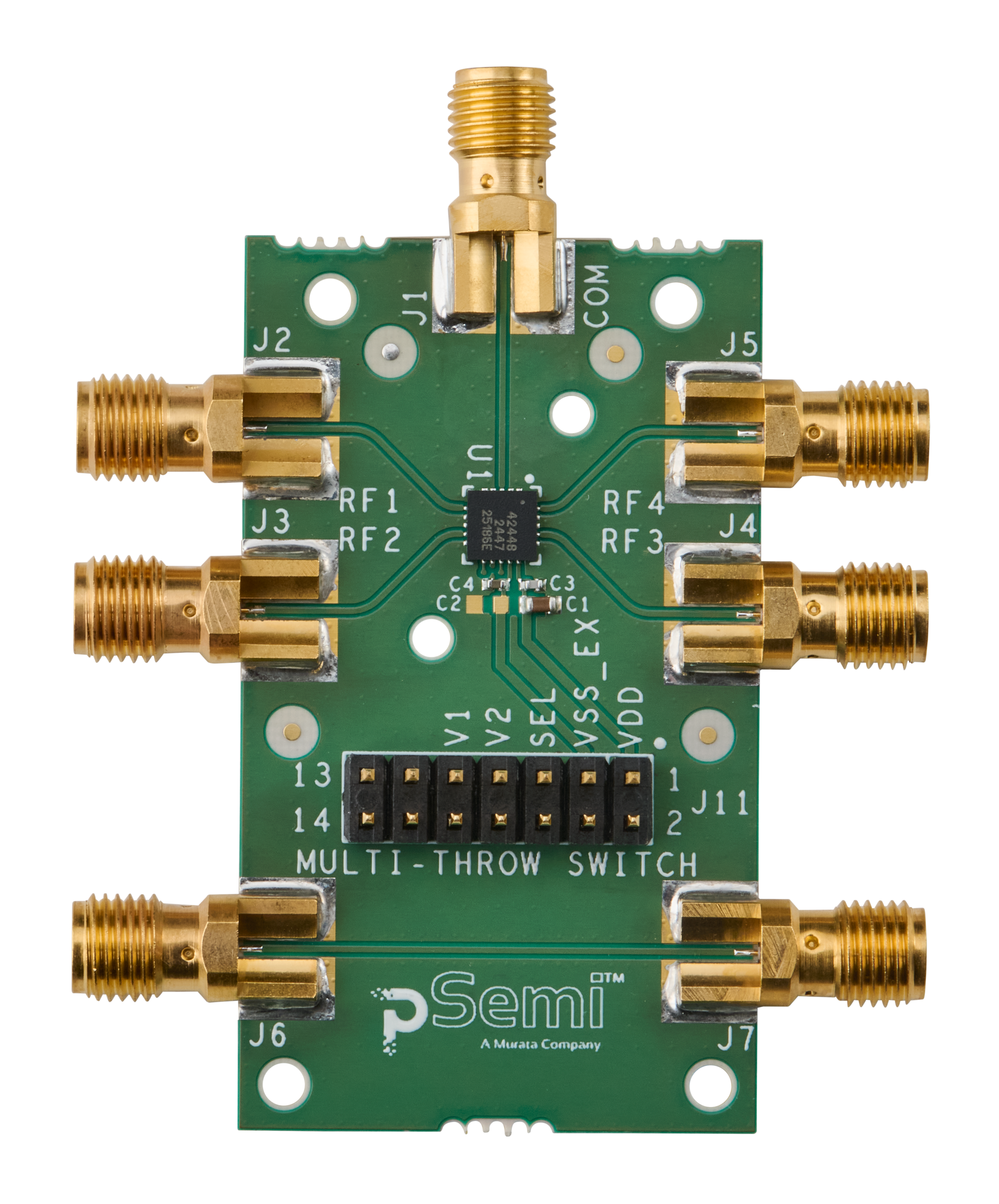 The PE42448 is a HaRP technology-enhanced SP4T RF switch that delivers extremely low insertion loss and high linearity with high input power handling capability. Source: pSemi
GS: pSemi has an impressive market portfolio, from personal electronics, military and defense solutions, to data centers and everything in between. Are innovations like UltraCMOS+ how you stay so ingrained in every corner of the RF world?
pSemi: Over the last 10 years, pSemi has not released UltraCMOS+ technology to our historical markets. During that time, we have focused our innovation on internal enablement of our parent company, Murata. Additionally, we have increased annual shipments from millions of units to billions of units. By aligning as one team with Murata, who ships trillions of units per year, we now have access to nearly every market and hold the status of a strategic supplier. As the head of marketing and sales, I am very excited to now release this technology and subsequent products to our historical customers, where instead of providing just switches, we can address the complete front end.
GS: How can our audience learn more about your technology?
pSemi: They can discover the perfect solutions by browsing our product pages and using our intuitive filters to compare specifications. Each product page also features a comprehensive library of technical resources to help dive deeper into the details.
They can also visit the news section of our website for press releases and blog articles that highlight our cutting-edge technology, and they can subscribe to our stay informed list to receive the latest news on new products and technologies, delivered straight to your inbox.
About pSemi
With a 35-year legacy of technology advancements, strong IP portfolio and deep expertise in RF integration, pSemi’s solution portfolio spans power management, connected sensors, antenna tuning and RF frontends, which enable advanced modules for smartphones, base stations, personal computers, electric vehicles, data centers, IoT devices, healthcare and more.


